IDT70V631S
High-Speed 3.3V 256K x 18 Asynchronous Dual-Port Static RAM Industrial and Commercial Temperature Ranges
18
Functional Description
The IDT70V631 provides two ports with separate control, address
and I/O pins that permit independent access for reads or writes to any
location in memory. The IDT70V631 has an automatic power down feature
controlled by CE. The CE0 and CE1 control the on-chip power down
circuitry that permits the respective port to go into a standby mode when
not selected (CE = HIGH). When a port is enabled, access to the entire
memory array is permitted.
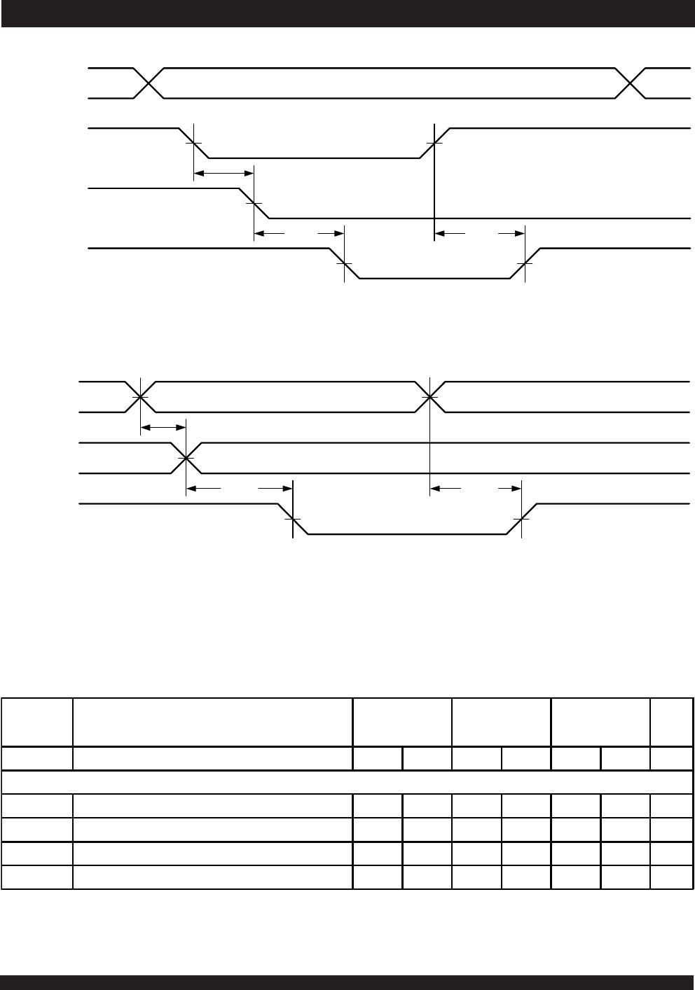
Interrupts
If the user chooses the interrupt function, a memory location (mail
box or message center) is assigned to each port. The left port interrupt
flag (INTL) is asserted when the right port writes to memory location
3FFFE (HEX), where a write is defined as CE
R = R/WR = VIL per the
Truth Table. The left port clears the interrupt through access of
address location 3FFFE when CEL = OEL = VIL, R/W is a "don't care".
Likewise, the right port interrupt flag (INTR) is asserted when the left
port writes to memory location 3FFFF (HEX) and to clear the interrupt
flag (INTR), the right port must read the memory location 3FFFF. The
message (18 bits) at 3FFFE or 3FFFF is user-defined since it is an
addressable SRAM location. If the interrupt function is not used,
address locations 3FFFE and 3FFFF are not used as mail boxes, but
as part of the random access memory. Refer to Truth Table III for
the interrupt operation.
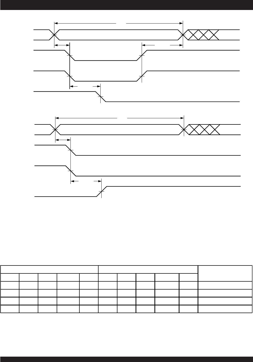
Truth Table IV —
Address BUSY Arbitration
NOTES:
1. Pins BUSY
L and BUSYR are both outputs when the part is configured as a master. Both are inputs when configured as a slave. BUSY outputs on the IDT70V631
are push-pull, not open drain outputs. On slaves the BUSY
input internally inhibits writes.
2. "L" if the inputs to the opposite port were stable prior to the address and enable inputs of this port. "H" if the inputs to the opposite port became stable after the address
and enable inputs of this port. If t
APS is not met, either BUSYL or BUSYR = LOW will result. BUSYL and BUSYR outputs can not be LOW simultaneously.
3. Writes to the left port are internally ignored when BUSY
L outputs are driving LOW regardless of actual logic level on the pin. Writes to the right port are internally ignored
when BUSY
R outputs are driving LOW regardless of actual logic level on the pin.
Truth Table V — Example of Semaphore Procurement Sequence
(1,2,3)
NOTES:
1. This table denotes a sequence of events for only one of the eight semaphores on the IDT70V631.
2. There are eight semaphore flags written to via I/O
0 and read from all I/O's (I/O0-I/O17). These eight semaphores are addressed by A0 - A2.
3. CE = V
IH, SEM = VIL to access the semaphores. Refer to the Semaphore Read/Write Control Truth Table.
Inputs Outputs
Function
CE
L
CE
R
A
OL
-A
17L
A
OR
-A
17R
BUSY
L
(1 )
BUSY
R
(1 )
X X NO MATCH H H Normal
H X MATCH H H Normal
X H MATCH H H Normal
LL MATCH (2) (2)
Write Inhibit
(3 )
5622 tbl 17
Functions D
0
- D
17
Left D
0
- D
17
Right Status
No Action 1 1 Semaphore free
Left Port Writes "0" to Semaphore 0 1 Left port has semaphore token
Right Port Writes "0" to Semaphore 0 1 No change. Right side has no write access to semaphore
Left Port Writes "1" to Semaphore 1 0 Right port obtains semaphore token
Left Port Writes "0" to Semaphore 1 0 No change. Left port has no write access to semaphore
Right Port Writes "1" to Semaphore 0 1 Left port obtains semaphore token
Left Port Writes "1" to Semaphore 1 1 Semaphore free
Right Port Writes "0" to Semaphore 1 0 Right port has semaphore token
Right Port Writes "1" to Semaphore 1 1 Semaphore free
Left Port Writes "0" to Semaphore 0 1 Left port has semaphore token
Left Port Writes "1" to Semaphore 1 1 Semaphore free
5622 tbl 18