LTC2927
1
2927fb
RAMP
(3.3V)
2.5V
1.8V
1V/DIV
2927 TA01b
10ms/DIV
RAMP
(3.3V)
2.5V
1.8V
1V/DIV
2927 TA01c
10ms/DIV
Single Power Supply
Tracking Controller
The LTC
®
2927 provides a simple solution to power supply
tracking and sequencing requirements. By selecting a few
resistors, the supply can be confi gured to ramp-up and
ramp-down with differing ramp rates, voltage offsets, or
time delays relative to other supplies or a master signal.
By forcing current into a feedback node of an independent
supply, the LTC2927 causes the output to track a ramp
signal without inserting any pass element losses. Because
the current is controlled in an open-loop manner, the
LTC2927 does not affect the transient response or stabil-
ity of the supply. The compact solution at point of load
minimizes the trace length of the DC/DC circuit sensitive
FB node. Furthermore, it presents a high impedance when
power-up is complete, effectively removing it from the
DC/DC circuit.
n
V
CORE
and V
I/O
Supply Tracking
n
Microprocessor, DSP and FPGA Supplies
n
Multiple Supply Systems
n
Point-of-Load Supplies
n
Flexible Power Supply Tracking
n
Tracks Both Up and Down
n
Power Supply Sequencing
n
Supply Stability is Not Affected
n
Low Pin Count
n
Controls Single Supply without Series FETs
n
Adjustable Ramp Rate
n
Supply Shutdown Output
n
Available in 8-Lead ThinSOT™ and 8-Lead
(3mm × 2mm) DFN Packages
138k
100k
ON RAMP
1.8V
V
CC
V
IN
EARLY V
IN
3.3V
LTC2927
GND
SDO RUN/SS
FB
IN
DC/DC
FB = 1.235V OUT
RAMPBUF
TRACK
0.1μF
16.5k
16.5k
35.7k
13k
ON RAMP
2.5V
2927 TA01a
V
CC
V
IN
EARLY V
IN
3.3V
LTC2927
GND
SDO RUN/SS
FB
IN
DC/DC
FB = 0.8V OUT
RAMPBUF
TRACK
0.1μF
0.1μF
887k
887k
412k
412k
, LT, LTC and LTM are registered trademarks of Linear Technology Corporation.
ThinSOT is a trademark of Linear Technology Corporation. All other trademarks are the
property of their respective owners. Patents Pending.
APPLICATIO S
U
FEATURES
DESCRIPTIO
U
TYPICAL APPLICATIO
U
Track-Up and Track-Down Waveforms
LTC2927
2
2927fb
Supply Voltage (V
CC
) ................................. –0.3V to 10V
Input Voltages
ON ......................................................... –0.3V to 10V
TRACK .........................................–0.3V to V
CC
+ 0.3V
Output Voltages
FB, SDO ................................................. –0.3V to 10V
RAMP, RAMPBUF .........................–0.3V to V
CC
+ 0.3V
(Note 1)
ABSOLUTE AXI U RATI GS
W
WW
U
Average Current
TRACK .................................................................5mA
FB ........................................................................5mA
RAMPBUF ............................................................5mA
Operating Temperature Range
LTC2927C ................................................ 0°C to 70°C
LTC2927I.............................................. –40°C to 85°C
Storage Temperature Range ................... –65°C to 150°C
Lead Temperature (Soldering, 10 sec) .................. 300°C
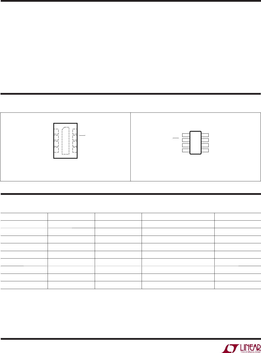
TOP VIEW
DDB PACKAGE
8-LEAD (3mm × 2mm) PLASTIC DFN
5
6
9
7
8
4
3
2
1ON
RAMP
RAMPBUF
TRACK
V
CC
SDO
FB
GND
EXPOSED PAD (PIN 9) PCB GND, CONNECTION OPTIONAL
T
JMAX
= 125°C, θ
JA
= 76°C/W
V
CC
1
SDO 2
FB 3
GND 4
8 ON
7 RAMP
6 RAMPBUF
5 TRACK
TOP VIEW
TS8 PACKAGE
8-LEAD PLASTIC TSOT-23
T
JMAX
= 125°C, θ
JA
= 250°C/W
PIN CONFIGURATION
ORDER INFORMATION
LEAD FREE FINISH TAPE AND REEL PART MARKING* PACKAGE DESCRIPTION TEMPERATURE RANGE
LTC2927CDDB#PBF LTC2927CDDB#TRPBF LBQH
8-Lead (3mm × 2mm) Plastic DFN
0°C to 70°C
LTC2927IDDB#PBF LTC2927IDDB#TRPBF LBQH
8-Lead (3mm × 2mm) Plastic DFN
–40°C to 85°C
LTC2927CTS8#PBF LTC2927CTS8#TRPBF LTBQJ 8-Lead Plastic TSOT-23 0°C to 70°C
LTC2927ITS8#PBF LTC2927ITS8#TRPBF LTBQJ 8-Lead Plastic TSOT-23 –40°C to 85°C
LEAD BASED FINISH TAPE AND REEL PART MARKING* PACKAGE DESCRIPTION TEMPERATURE RANGE
LTC2927CDDB LTC2927CDDB#TR LBQH
8-Lead (3mm × 2mm) Plastic DFN
0°C to 70°C
LTC2927IDDB LTC2927IDDB#TR LBQH
8-Lead (3mm × 2mm) Plastic DFN
–40°C to 85°C
LTC2927CTS8 LTC2927CTS8#TR LTBQJ 8-Lead Plastic TSOT-23 0°C to 70°C
LTC2927ITS8 LTC2927ITS8#TR LTBQJ 8-Lead Plastic TSOT-23 –40°C to 85°C
Consult LTC Marketing for parts specifi ed with wider operating temperature ranges. *The temperature grade is identifi ed by a label on the shipping container.
For more information on lead free part marking, go to:
http://www.linear.com/leadfree/
For more information on tape and reel specifi cations, go to:
http://www.linear.com/tapeandreel/
LTC2927
3
2927fb
TEMPERATURE (°C)
–50
770
V
TRACK
(mV)
780
790
800
810
820
–25 0 25 50
2927 G03
75 100
V
CC
(V)
4.45
I
CC
(mA)
4.50
4.55
4.60
4.65
4.70
2927 G0
2
2.5 3.0 3.5 4.0 4.5 6.
0
5.55.0
I
TRACK
= I
FB
= –1mA
I
RAMBUF
= –2mA
V
CC
(V)
2.5
500
I
CC
(μA)
550
600
650
700
750
3.0 3.5 4.0 4.5
2927 G0
1
6.05.55.0
I
TRACK
= I
FB
= 0mA
I
RAMBUF
= 0mA
I
CC
vs V
CC
I
CC
vs V
CC
V
TRACK
vs Temperature
The
l denotes the specifi cations which apply over the full operating
temperature range, otherwise specifi cations are at T
A
= 25°C. 2.9V < V
CC
< 5.5V unless otherwise noted (Note 2).
Note 1: Stresses beyond those listed under Absolute Maximum Ratings
may cause permanent damage to the device. Exposure to any Absolute
Maximum Rating condition for extended periods may affect device
reliability and lifetime.
Note 2: All currents into the device pins are positive; all currents out of
device pins are negative. All voltages are referenced to ground unless
otherwise specifi ed.
SYMBOL PARAMETER CONDITIONS MIN TYP MAX UNITS
V
CC
Supply Voltage
l
2.9 5.5 V
I
CC
Supply Current I
FB
= 0mA, I
TRACK
= 0mA
l
0.25 0.56 1.2 mA
I
FB
= –1mA, I
TRACK
= –1mA, I
RAMPBUF
= –1mA
l
3 3.6 4.2 mA
V
CC(UVLO)
Supply Undervoltage Lockout V
CC
Rising
l
2.2 2.5 2.7 V
ΔV
CC(UVHYST)
Supply Undervoltage Lockout Hysteresis 25 mV
V
ON(TH)
ON Pin Threshold Voltage V
ON
Rising
l
1.210 1.230 1.250 V
ΔV
ON(HYST)
ON Pin Hysteresis
l
30 75 150 mV
I
ON
ON Pin Input Current V
ON
= 1.2V, V
CC
= 5.5V
l
0 ±100 nA
I
RAMP
RAMP Pin Input Current 0V < V
RAMP
< V
CC
, Ramp On –9 –10 –11 μA
0V < V
RAMP
< V
CC
, Ramp Off 9 10 11 μA
V
RAMPBUF(OL)
RAMPBUF Output Low Voltage I
RAMPBUF
= 1mA
l
20 100 mV
V
RAMPBUF(OH)
RAMPBUF Output High Voltage,
V
RAMPBUF(OH)
= V
CC
– V
RAMPBUF
I
RAMPBUF
= –1mA
l
45 150 mV
V
OS
Ramp Buffer Offset,
V
OS
= V
RAMPBUF
– V
RAMP
V
RAMP
= V
CC
/2, I
RAMPBUF
= 0mA –30 0 30 mV
I
ERROR(%)
I
FB
to I
TRACK
Current Mismatch
I
ERROR(%)
= (I
FB
– I
TRACK
)/I
TRACK
I
TRACK
= –10μA
l
5 %
I
TRACK
= –1mA
l
5 %
V
TRACK
TRACK Pin Voltage I
TRACK
= –10μA
l
0.77 0.800 0.82 V
I
TRACK
= –1mA
l
0.77 0.800 0.82 V
I
FB(LEAK)
FB Pin Leakage Current V
FB
= 2V, V
CC
= 5.5V
l
±1 ±100 nA
V
FB(CLAMP)
FB Pin Clamp Voltage 1μA < I
FB
< 1mA
l
1.5 2 2.3 V
V
SDO(OL)
SDO Output Low Voltage I
SDO
= 1mA, V
CC
= 2.3V
l
0.1 0.4 V
ELECTRICAL CHARACTERISTICS
TYPICAL PERFORMANCE CHARACTERISTICS

LTC2927IDDB#TRPBF

Mfr. #:
Manufacturer:
Analog Devices Inc.
Description:
Power Management Specialized - PMIC 1x Pwr S Track Cntr
Lifecycle:
New from this manufacturer.
Delivery:
DHL FedEx Ups TNT EMS
Payment:
T/T Paypal Visa MoneyGram Western Union