LTC2927
13
2927fb
Final Sanity Checks
The collection of equations below is useful for identifying
unrealizable solutions.
As stated in step 2, the slave supply must fi nish ramping
before the master signal has reached its fi nal voltage. This
can be verifi ed by the following equation:
V
R
R
V
TRACK
TB
TA
MASTER
1+
<
Here, V
TRACK
= 0.8V. V
MASTER
is the fi nal voltage of the
master signal (V
CC
if RAMP pin).
It is possible to choose resistor values that require the
LTC2927 to supply more current than the Electrical Char-
acteristics table guarantees. To avoid this condition, check
that I
TRACK
does not exceed 1mA and I
RAMPBUF
does not
exceed ±2mA.
To confi rm that I
TRACK
< 1mA, the TRACK pin’s maximum
guaranteed current, verify that:
V
RR
mA
TRACK
TA TB
< 1
Finally, check that the RAMPBUF pin will not be forced to
sink more than 2mA when it is at 0V or be forced to source
more than 2mA when it is at V
MASTER
.
V
R
mA and
V
RR
mA
TRACK
TB
MASTER
TA TB
<
+
<22
ON Pin Resistive Divider
Check that the ON pin voltage is above the 1.25V maximum
threshold at the lowest possible supply voltage value.
R
R
V
V
ONB
ONA
CC MIN
<
()
.
125
1
Also check that the supply voltage is above the minimum
LTC2927 operating supply voltage of 2.9V before the ON
pin is above the 1.21V minimum threshold voltage.
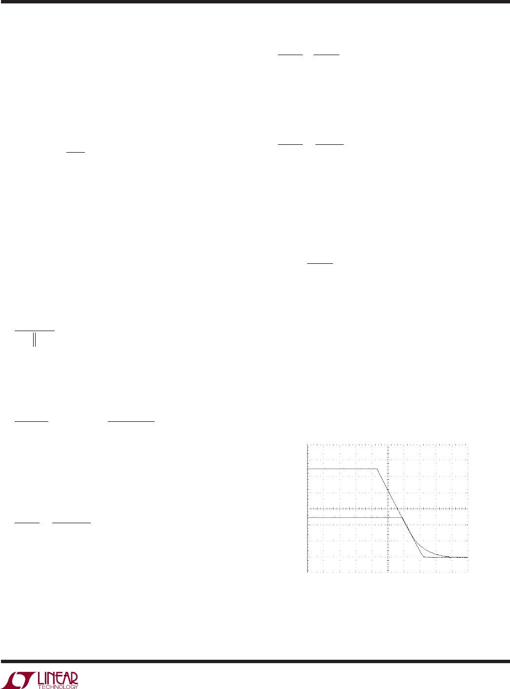
Figure 17. Weak Resistive Load
2927 F17
10ms/DIV
1V/DIV
MASTER
SLAVE
R
R
V
V
ONB
ONA
<
29
121
1
.
.
For example, if the typical application shown on page 1
has a 3.3V ±10% V
IN
, the lowest possible operating supply
voltage will be 2.97.
R
R
V
V
ONB
ONA
>=
297
125
1 1 376
.
.
–.
If R
ONA
is 100k then R
ONB
must be greater than 137.6k.
Therefore, 138k is chosen. These values must be checked
to ensure the supply reaches the LTC2927 minimum op-
erating supply voltage of 2.9V before the ON pin is above
the minimum threshold.
138
29
121
1 1 389.
.
.
–.<=
V
V
Load Requirements
When the supply is ramped down quickly, either the load
or the supply itself must be capable of sinking enough
current to support the ramp rate. For example, if there
is a large output capacitance on the supply and a weak
resistive load, supplies that do not sink current will have
their falling ramp rate limited by the RC time constant of
the load and the output capacitance. Figure 17 shows the
case when the slave supply does not track the master
near ground.
APPLICATIO S I FOR ATIO
WUU
U
LTC2927
14
2927fb
Start-Up Delays
Often power supplies do not start-up immediately when
their input supplies are applied. If the LTC2927 tries to
ramp-up these power supplies as soon as the input sup-
ply is present, the start-up of the outputs may be delayed,
defeating the tracking circuit (Figure 18). Often this delay is
intentionally confi gured by a soft-start capacitor. This can
be remedied either by reducing the soft-start capacitor on
the slave supply or by including a capacitor in the ON pin’s
resistive divider to delay the ramp up. See Figure 19.
Figure 20. Layout Considerations
Layout Considerations
Be sure to place a 0.1μF bypass capacitor as near as pos-
sible to the supply pin of the LTC2927.
To minimize the noise on the slave supplys output, keep
the trace connecting the FB pin of the LTC2927 and the
feedback node of the slave supply as short as possible.
In addition, do not route this trace next to signals with
fast transition times. In some circumstances it might be
advantageous to add a resistor near the feedback node of
the slave supply in series with the FB pin of the LTC2927.
This resistor must not exceed:
R
VV
I
V
V
RR
SERIES
FB
MAX FB
FA FB
=
=−
()
15 15
1
..
This resistor is most effective if there is already a ca-
pacitor at the feedback node of the slave supply (often a
compensation component). Increasing the capacitance on
a slave supplys feedback node will further improve the
noise immunity, but could affect the stability and transient
response of the supply.
V
CC
2927 F20
LTC2927
FB
GND
DC/DC
FB OUT
0.1μF
MINIMIZE
TRACE
LENGTH
R
FB
R
FA
R
SERIES
APPLICATIO S I FOR ATIO
WUU
U
Figure 18. Power Supply Start-Up Delayed
Figure 19. ON Pin Delayed
2927 F18
1V/DIV
20ms/DIV
MASTER
SLAVE
ON
2927 F19
1V/DIV
5ms/DIV
MASTER
SLAVE
ON
LTC2927
15
2927fb
Information furnished by Linear Technology Corporation is believed to be accurate and reliable.
However,
no responsibility is assumed for its use. Linear Technology Corporation makes no representation that
the interconnection of its circuits as described herein will not infringe on existing patent rights.
DDB Package
8-Lead Plastic DFN (3mm × 2mm)
(Reference LTC DWG # 05-08-1702)
2.00 ±0.10
(2 SIDES)
NOTE:
1. DRAWING CONFORMS TO VERSION (WECD-1) IN JEDEC PACKAGE OUTLINE M0-229
2. DRAWING NOT TO SCALE
3. ALL DIMENSIONS ARE IN MILLIMETERS
4. DIMENSIONS OF EXPOSED PAD ON BOTTOM OF PACKAGE DO NOT INCLUDE
MOLD FLASH. MOLD FLASH, IF PRESENT, SHALL NOT EXCEED 0.15mm ON ANY SIDE
5. EXPOSED PAD SHALL BE SOLDER PLATED
6. SHADED AREA IS ONLY A REFERENCE FOR PIN 1 LOCATION ON THE TOP AND BOTTOM OF PACKAGE
0.38 ± 0.10
BOTTOM VIEW—EXPOSED PAD
0.56 ± 0.05
(2 SIDES)
0.75 ±0.05
R = 0.115
TYP
2.15 ±0.05
(2 SIDES)
3.00 ±0.10
(2 SIDES)
14
85
PIN 1 BAR
TOP MARK
(SEE NOTE 6)
0.200 REF
0 – 0.05
(DDB8) DFN 1103
0.25 ± 0.05
2.20 ±0.05
(2 SIDES)
RECOMMENDED SOLDER PAD PITCH AND DIMENSIONS
0.61 ±0.05
(2 SIDES)
1.15 ±0.05
0.675 ±0.05
2.50 ±0.05
PACKAGE
OUTLINE
0.25 ± 0.05
0.50 BSC
PIN 1
CHAMFER OF
EXPOSED PAD
0.50 BSC
1.50 – 1.75
(NOTE 4)
2.80 BSC
0.22 – 0.36
8 PLCS (NOTE 3)
DATUM ‘A’
0.09 – 0.20
(NOTE 3)
TS8 TSOT-23 0802
2.90 BSC
(NOTE 4)
0.65 BSC
1.95 BSC
0.80 – 0.90
1.00 MAX
0.01 – 0.10
0.20 BSC
0.30 – 0.50 REF
PIN ONE ID
NOTE:
1. DIMENSIONS ARE IN MILLIMETERS
2. DRAWING NOT TO SCALE
3. DIMENSIONS ARE INCLUSIVE OF PLATING
4. DIMENSIONS ARE EXCLUSIVE OF MOLD FLASH AND METAL BURR
5. MOLD FLASH SHALL NOT EXCEED 0.254mm
6. JEDEC PACKAGE REFERENCE IS MO-193
3.85 MAX
0.52
MAX
0.65
REF
RECOMMENDED SOLDER PAD LAYOUT
PER IPC CALCULATOR
1.4 MIN
2.62 REF
1.22 REF
TS8 Package
8-Lead Plastic TSOT-23
(Reference LTC DWG # 05-08-1637)
PACKAGE DESCRIPTIO
U

LTC2927IDDB#TRPBF

Mfr. #:
Manufacturer:
Analog Devices Inc.
Description:
Power Management Specialized - PMIC 1x Pwr S Track Cntr
Lifecycle:
New from this manufacturer.
Delivery:
DHL FedEx Ups TNT EMS
Payment:
T/T Paypal Visa MoneyGram Western Union