LTC2927
10
2927fb
This example converts the coincident tracking example to
the ratiometric tracking profi le shown in Figure 11. The
ramp rate of the master signal remains unchanged (Step
1) and there is no delay in ratiometric tracking (Step 3),
so only the result of step 2 in the 3-step design procedure
needs to be considered. In this example, the ramp rate of the
1.8V slave 1 supply ramps up at 60V/s and the 2.5V slave 2
supply ramps up at 85V/s. Always verify that the chosen
ramp rate will allow the supplies to ramp-up completely
before RAMPBUF reaches V
CC
. If the 1.8V supply were
to ramp-up at 50V/s it would only reach 1.65V because
the RAMPBUF signal would reach its fi nal value of V
CC
=
3.3V before the slave supply reached 1.8V.
2. Solve for the pair of resistors that provide the desired
slave supply behavior, assuming no delay.
From Equation 2:
Rk
Vs
Vs
k
TB
=• =16 5
100
60
27 4.
/
/
.ΩΩ
From Equation 3:
R
V
V
k
V
k
V
k
k
TA
=
+−
08
1 235
16 5
1 235
35 7
08
27 4
10
.
.
.
.
.
.
.ΩΩΩ
Ω
Step 3 is unnecessary because there is no delay, so
R
TA
= R
TA
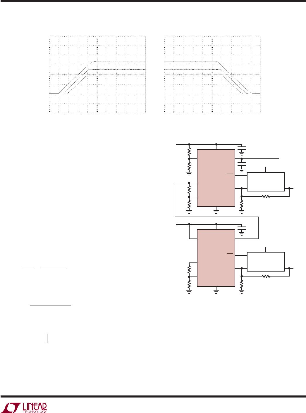
Figure 11. Ratiometric Tracking (from Figure 12)
1V/DIV
10ms/DIV
SLAVE1
MASTER
SLAVE2
2927 F11
10ms/DIV
1V/DIV
MASTER
3.3V
R
ONB
138k
R
ONA
100k
ON RAMP
SLAVE1
1.8V
V
CC
3.3V
EARLY V
IN
3.3V
LTC2927
GND
SDO RUN/SS
FB
IN
DC/DC
FB = 1.235V OUT
RAMPBUF
TRACK
0.1μF
R
TB1
27.4k
R
FB1
16.5k
R
FA1
35.7k
R
TA1
10k
ON RAMP
SLAVE2
2.5V
2927 F12
V
CC
3.3V
EARLY
3.3V
LTC2927
GND
SDO RUN/SS
FB
IN
DC/DC
FB = 0.8V OUT
RAMPBUF
TRACK
0.1μF
0.1μF
R
TB2
1M
R
FB2
887k
R
FA2
412k
R
TA2
383k
Ratiometric Tracking Example
APPLICATIO S I FOR ATIO
WUU
U
Figure 12. Ratiometric Tracking Example
LTC2927
11
2927fb
Converting the circuit in the coincident tracking example
to the offset tracking shown in Figure 13 is relatively
simple. Here the 1.8V slave 1 supply ramps up 1V below
the master. The ramp rate remains the same (100V/s), so
there are no changes necessary to steps 1 and 2 of the
3-step design procedure. Only step 3 must be considered.
Be sure to verify that the chosen voltage offset will allow
the slave supply to ramp up completely. In this example,
if the voltage offset were 2V, the slave supply would only
ramp to 3.3V – 2V = 1.3V.
3. Choose R
TA
to obtain desired delay.
First, convert the desired voltage offset, V
OS
, to a delay
t
D
, using the ramp rate:
t
V
S
V
Vs
ms
D
OS
S
== =
1
100
10 6
/
()
From Equation 4:
R
Vk
ms V s
k
TA
=
=
0 8 16 5
10 100
13 2
..
/
.
Ω
Ω
From Equation 5:
Rkkk
TA
=≈131 132 665.. .ΩΩ Ω
Figure 13. Offset Tracking (from Figure 14)
1V/DIV
10ms/DIV
MASTER
SLAVE1
SLAVE2
2927 F13
10ms/DIV
1V/DIV
MASTER
3.3V
R
ONB
138k
R
ONA
100k
ON RAMP
SLAVE1
1.8V
V
CC
3.3V
EARLY V
IN
3.3V
LTC2927
GND
SDO RUN/SS
FB
IN
DC/DC
FB = 1.235V OUT
RAMPBUF
TRACK
0.1μF
R
TB1
16.5k
R
FB1
16.5k
R
FA1
35.7k
R
TA1
6.65k
ON RAMP
SLAVE2
2.5V
2927 F14
V
CC
3.3V
EARLY
3.3V
LTC2927
GND
SDO RUN/SS
FB
IN
DC/DC
FB = 0.8V OUT
RAMPBUF
TRACK
0.1μF
0.1μF
R
TB2
887k
R
FB2
887k
R
FA2
412k
R
TA2
316k
Offset Tracking Example
APPLICATIO S I FOR ATIO
WUU
U
Figure 14. Offset Tracking Example
LTC2927
12
2927fb
Figure 15. Supply Sequencing (from Figure 16)
Figure 16. Supply Sequencing Example
1V/DIV
10ms/DIV
MASTER
SLAVE1
SLAVE2
2927 F15
10ms/DIV
1V/DIV
MASTER
3.3V
R
ONB
138k
R
ONA
100k
ON RAMP
SLAVE1
1.8V
V
CC
3.3V
EARLY V
IN
3.3V
LTC2927
GND
SDO RUN/SS
FB
IN
DC/DC
FB = 1.235V OUT
RAMPBUF
TRACK
0.1μF
R
TB1
1.65k
R
FB1
16.5k
R
FA1
35.7k
R
TA1
3.48k
ON RAMP
SLAVE2
2.5V
2927 F16
V
CC
3.3V
EARLY
3.3V
LTC2927
GND
SDO RUN/SS
FB
IN
DC/DC
FB = 0.8V OUT
RAMPBUF
TRACK
0.1μF
0.1μF
R
TB2
88.7k
R
FB2
887k
R
FA2
412k
R
TA2
36.5k
In Figure 15, the slave 1 supply and the slave 2 supply are
sequenced instead of tracking. The 3.3V master ramps up
at 100V/s. The 1.8V slave 1 supply ramps up at 1000V/s
beginning 10ms after the master signal starts to ramp up.
The 2.5V slave 2 supply ramps up at 1000V/s beginning
25ms after the master signal begins to ramp up. Note
that not every combination of ramp rates and delays is
possible. Small delays and large ratios of slave ramp rate
to master ramp rate may result in solutions that require
negative resistors. In such cases, either the delay must
be increased or the ratio of slave ramp rate to master
ramp rate must be reduced. In this example, solving for
the slave supply yields:
1. Set the ramp rate of the master signal.
From Equation 1:
C
A
Vs
F
RAMP
==μ
10
100
01
μ
/
.
2. Solve for the pair of resistors that provide the desired
slave supply behavior, assuming no delay.
Rk
Vs
Vs
k
TB
=• =16 5
100
1000
165.
/
/
.ΩΩ
From Equation 3:
R
V
V
k
V
k
V
k
k
TA
=
+−
=−
08
1 235
16 5
1 235
35 7
08
165
213
.
.
.
.
.
.
.
.
ΩΩΩ
Ω
3. Choose R
TA
to obtain desired delay.
From Equation 4:
R
Vk
ms V s
k
TA
=
=
08 165
10 100
132
..
/
.
Ω
Ω
From Equation 5:
Rkkk
TA
=− =213 132 348.. .ΩΩ Ω
Supply Sequencing Example
APPLICATIO S I FOR ATIO
WUU
U

LTC2927IDDB#TRPBF

Mfr. #:
Manufacturer:
Analog Devices Inc.
Description:
Power Management Specialized - PMIC 1x Pwr S Track Cntr
Lifecycle:
New from this manufacturer.
Delivery:
DHL FedEx Ups TNT EMS
Payment:
T/T Paypal Visa MoneyGram Western Union