LTC5598
10
5598f
APPLICATIONS INFORMATION
be the signal source for the LTC5598. A reconstruction
fi lter should be placed between the DAC output and the
LTC5598’s baseband inputs.
In Figure 2 a typical baseband interface is shown, using
a fi fth-order lowpass ladder fi lter.
in Table 3. In Table 4 and 5, the LOP port input impedance
is given for EN = High and Low under the condition of
P
LO
= 10dBm. Figure 4 shows the LOP port return loss
for the standard demo board (schematic is shown in
Figure 10) when the LOM port is terminated with 50Ω to
GND. The values of L1, L2, C9 and C10 are chosen such
that the bandwidth for the LOP port of the standard demo
board is maximized while meeting the LO input return loss
S
11, ON
< –10dB.
Table 2. LOP Port Input Impedance vs Frequency for EN = High
and P
LO
= 0dBm (LOM AC Coupled With 50Ω to Ground).
FREQUENCY
(MHz)
LO INPUT
IMPEDANCE
REFLECTION COEFFICIENT
MAG ANGLE
0.1 333 – j10.0 0.739 –0.5
1 318 – j59.9 0.737 –3.3
2 285 – j94.7 0.728 –6.1
4 227 – j120 0.708 –10.6
8 154 – j124 0.678 –18.7
16 89.9 – j95.4 0.611 –33.0
30 60.4 – j60.6 0.420 –41.3
60 54.8 – j35.8 0.489 –51.5
100 43.6 – j24.4 0.261 –89.9
200 37.9 – j17.3 0.235 –113
400 31.8 – j12.4 0.266 –137
800 23.6 – j8.2 0.374 –156
1000 19.8 – j5.5 0.437 –165
1250 16.0 – j1.8 0.515 –175
1500 13.6 + j2.4 0.574 174
1800 12.1 + j7.3 0.618 162
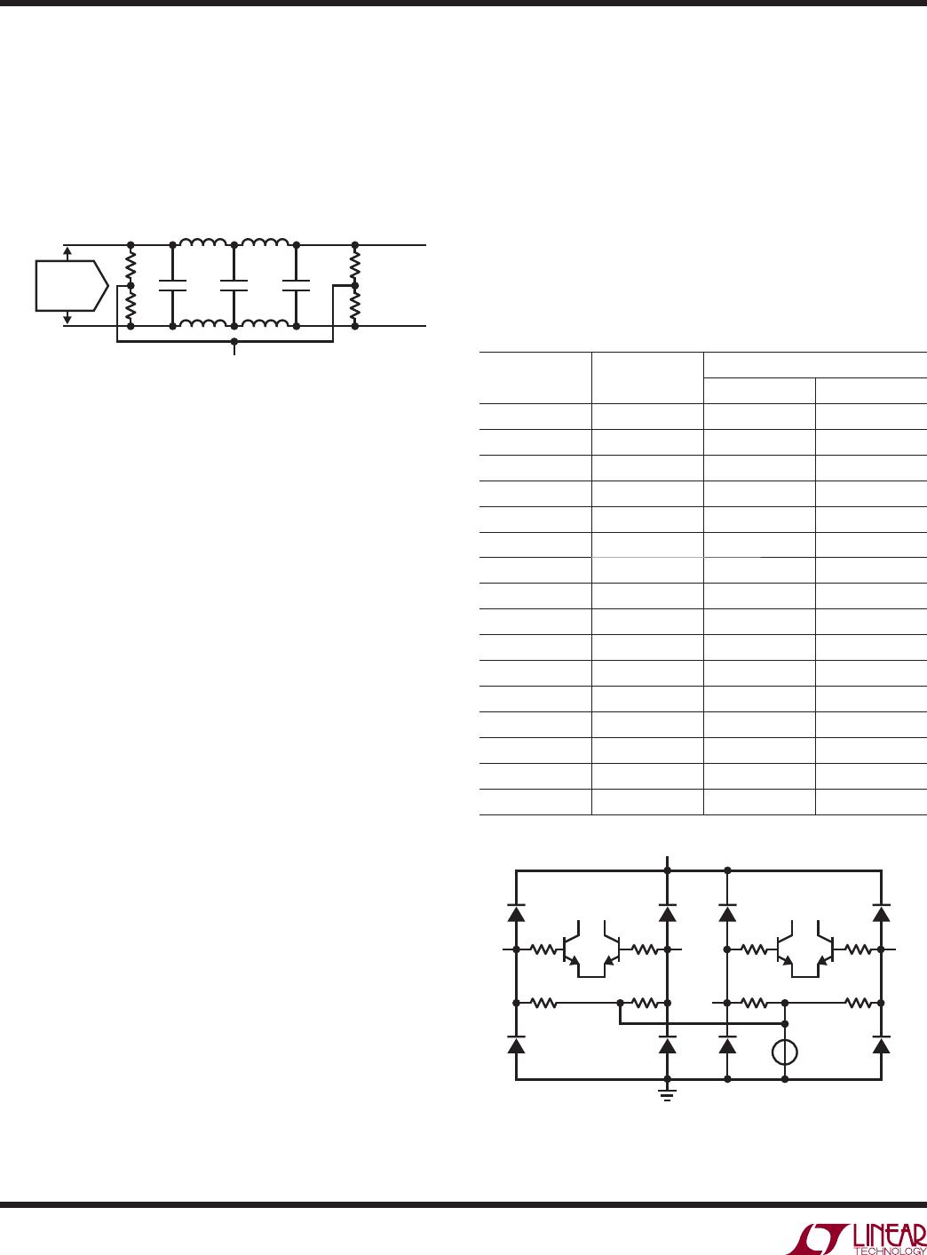
BBPI
R2A
1007
L2A
L2B
GND
0.5V
DC
0.5V
DC
C3
R2B
1007
BBMI
5598 F02
R1A
1007
R1B
1007
L1A
L1B
C2
C1
DAC
0mA TO 20mA
0mA TO 20mA
Figure 2. Baseband Interface with 5th Order Filter
and 0.5V
CM
DAC (Only I Channel is Shown)
For each baseband pin, a 0 to 1V swing is developed
corresponding to a DAC output current of 0mA to 20mA.
The maximum sinusoidal single side-band RF output power
is about +7.3dBm for full 0V to 1V swing on each I- and
Q- channel baseband input (2V
PP, DIFF
).
LO Section
The internal LO chain consists of poly-phase phase shifters
followed by LO buffers. The LOP input is designed as a
single-ended input with about 50Ω input impedance. The
LOM input should be terminated with 50Ω through a DC
blocking capacitor.
The LOP and LOM inputs can be driven differentially in
case an exceptionally low large-signal output noise fl oor
is required (see graph 5598 G20b).
A simplifi ed circuit schematic for the LOP, LOM, CAPA
and CAPB inputs is given in Figure 3. A feedback path is
implemented from the LO buffer outputs to the LO inputs
in order to minimize offsets in the LO chain by storing the
offsets on C5, C7 and C8 (see Figure 10). Optional capacitor
C8 improves the image rejection below 100MHz (see
graph 5598 G20a). Because of the feedback path, the input
impedance for P
LO
= 0dBm is somewhat different than
for P
LO
= 10dBm for the lower part of the operating
frequency range. In Table 2, the LOP port input impedance
vs frequency is given for EN = High and P
LO
= 0dBm. For
EN = Low and P
LO
= 0dBm, the input impedance is given
V
CC1
2.8V
(4.3V IN
SHUTDOWN)
LOP LOM
CAPA
CAPB
5598 F03
+
Figure 3. Simplifi ed Circuit Schematic for the
LOP, LOM, CAPA and CAPB Inputs.

