LTC5598
7
5598f
Noise Floor vs RF Frequency
(P
LO
= 10dBm, No AC Baseband
Input Signal)
Image Rejection DistributionLO Feedthrough Distribution
Gain Distribution
LO Feedthrough to RF Output
vs LO Frequency for EN = Low
Output IP3 Distribution at 25°C
TYPICAL PERFORMANCE CHARACTERISTICS
V
CC
= 5V, EN = 5V, T
A
= 25ºC, f
RF
= f
LO
– f
BB
, f
LO =
450MHz, P
LO
= 0dBm single-ended, BBPI, BBMI, BBPQ, BBMQ common-mode DC voltage V
CMBB
= 0.5V
DC
, I&Q baseband input signal
= 100kHz, 0.8V
PP,DIFF
, two-tone baseband input signal = 2MHz, 2.1MHz, 0.5V
PP,DIFF
each tone, I&Q 90° shifted (lower side-band
selection); f
NOISE
= f
LO
– 6MHz; unless otherwise noted. (Note 11)
RF FREQUENCY (MHz)
NOISE FLOOR (dBm/Hz)
–145
–150
–155
–160
–165
5598 G19
100010010
5V, 25°C
5.25V, 25°C
4.5V, 25°C
5V, –40°C
5V, 85°C
(NOTE 3)
LO FREQUENCY (MHz)
LO FEEDTHROUGH (dBm)
–40
–80
–60
–100
–120
–140
5598 G20
100010010
P
LO
= 10dBm
P
LO
= 0dBm
–40°C
85°C
GAIN (dB)
PERCENTAGE (%)
60
50
40
30
20
10
0
5598 G21
–1.9–2–2.2 –2.1–2.3–2.4
85oC
25oC
–40oC
OIP3 (dBm)
PERCENTAGE (%)
30
25
20
10
15
5
0
5598 G22
26.8 27.225.6 26 26.424.8 25.224.424
LO FEEDTHROUGH (dBm)
PERCENTAGE (%)
25
20
15
10
5
0
5598 G23
–42 –38–54 –50 –46–62 –58–66–70
85oC
25oC
–40oC
IMAGE REJECTION (dBc)
PERCENTAGE (%)
40
35
30
20
25
15
10
5
0
5598 G24
–42–46–62 –58 –54 –50–66–70
85oC
25oC
–40oC
NOISE FLOOR (dBm/Hz)
PERCENTAGE (%)
70
60
50
20
40
30
10
0
5598 G25
–160.4 –160–161.2 –160.8–161.6–162–162.4
85oC
25oC
–40oC
NO RF
Noise Floor Distribution
LO FREQUENCY (MHz)
IMAGE REJECTION (dBc)
0
–80
–70
–60
–50
–40
–30
–20
–10
5598 G20a
100010010
C8 = 0
C8 = 470nF
Image Rejection vs LO Frequency
(P
LO
= 10dBm)
RF OUTPUT POWER (dBm)
NOISE FLOOR AT 6MHz OFFSET (dBm/Hz)
–152
–154
–156
–160
–158
–162
5598 G20b
86420–2–4–6–8–10–12–14
20dBm
19.3dBm
13.4dBm
10.4dBm
8.4dBm
6.4dBm
f
LO
= 140MHz; f
BB
= 2kHz; CW (NOTE 3)
Noise Floor vs RF Output Power and
Differential LO Input Power
LTC5598
8
5598f
BLOCK DIAGRAM
PIN FUNCTIONS
EN (Pin 1): Enable Input. When the Enable Pin voltage is
higher than 2 V, the IC is turned on. When the input voltage
is less than 1 V, the IC is turned off. If not connected, the
IC is enabled.
GND (Pins 2, 5, 8, 11, 12, 19, 20, 23 and 25): Ground.
Pins 2, 5, 8, 11, 12, 19, 20, 23 and exposed pad 25 are
connected to each other internally. For best RF performance,
pins 2, 5, 8, 11, 12, 19, 20, 23 and the Exposed Pad 25
should be connected to RF ground.
LOP (Pin 3): Positive LO Input. This LO input is internally
biased at about 2.3V. An AC de-coupling capacitor should
be used at this pin to match to an external 50Ω source.
LOM (Pin 4): Negative LO Input. This input is internally biased
at about 2.3V. An AC de-coupling capacitor should be used at
this pin via a 50Ω to ground for best OIP2 performance.
CAPA, CAPB (Pins 6, 7): External capacitor pins. A cap-
acitor between the CAPA and the CAPB pin can be used in
order to improve the image rejection for frequencies below
100MHz. A capacitor value of 470nF is recommended.
These pins are internally biased at about 2.3V.
BBMQ, BBPQ (Pins 9, 10): Baseband Inputs for the
Q-channel, each high input impedance. They should be
externally biased at 0.5V common-mode level and not be
left fl oating. Applied common-mode voltage must stay
below 0.6V
DC
.
NC (Pins 13, 15): No Connect. These pins are fl oating.
GNDRF (Pins 14, 17): Ground. Pins 14 and 17 are connected
to each other internally and function as the ground return for
the RF output buffer. They are connected via back-to-back
diodes to the exposed pad 25. For best LO suppression
performance those pins should be grounded separately
from the exposed paddle 25. For best RF performance,
pins 14 and 17 should be connected to RF ground.
RF (Pin 16): RF Output. The RF output is a DC-coupled
single-ended output with approximately 50Ω output
impedance at RF frequencies. An AC coupling capacitor
should be used at this pin to connect to an external
load.
V
CC
(Pins 18, 24): Power Supply. It is recommended to
use 1nF and 4.7μF capacitors for decoupling to ground
on each of these pins.
BBPI, BBMI (Pins 21, 22): Baseband Inputs for the Q-
channel, each high input impedance. They should be
externally biased at 0.5V common-mode level and not be
left fl oating. Applied common-mode voltage must stay
below 0.6V
DC
.
Exposed Pad (Pin 25): Ground. This pin must be soldered
to the printed circuit board ground plane.
90o
0o
LTC5598
V-I
V-I
RF
GNDRF
LOP LOM CAPA CAPB
16
EN
1
3118
GND
52
9
10
22
21
24 18
NC
13 15
BBPI
BBMI
BBPQ
BBMQ
252320
GND
764
5598 BD
19
17
GND
14
12
V
CC1
V
CC2
LTC5598
9
5598f
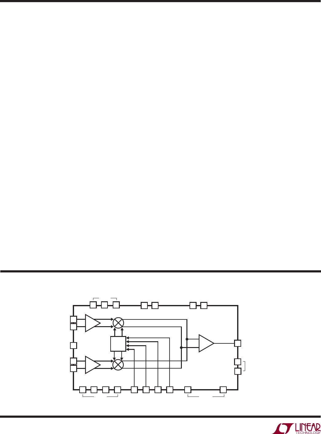
The LTC5598 consists of I and Q input differential voltage-
to-current converters, I and Q up-conversion mixers, an
RF output buffer, an LO quadrature phase generator and
LO buffers.
External I and Q baseband signals are applied to the
differential baseband input pins, BBPI, BBMI, and BBPQ,
BBMQ. These voltage signals are converted to currents and
translated to RF frequency by means of double-balanced
up-converting mixers. The mixer outputs are combined
in an RF output buffer, which also transforms the output
impedance to 50Ω. The center frequency of the resulting
RF signal is equal to the LO signal frequency. The LO input
drives a phase shifter which splits the LO signal into in-
phase and quadrature LO signals. These LO signals are then
applied to on-chip buffers which drive the up-conversion
mixers. In most applications, the LOP input is driven by
the LO source via an optional matching network, while
the LOM input is terminated with 50Ω to RF ground via
a similar optional matching network. The RF output is
single-ended and internally 50Ω matched.
Baseband Interface
The circuit is optimized for a common mode voltage of
0.5V which should be externally applied. The baseband
pins should not be left fl oating because the internal
PNPs base current will pull the common mode voltage
higher than the 0.6V limit. This condition may damage
the part. In shut-down mode, it is recommended to have
a termination to ground or to a 0.5V source with a value
lower than 1kΩ. The PNPs base current is about –68μA
in normal operation.
The baseband inputs (BBPI, BBMI, BBPQ, BBMQ) present
a single-ended input impedance of about –7.4kΩ each.
Because of the negative input impedance, it is important
to keep the source resistance at each baseband input low
enough such that the parallel value remains positive vs
baseband frequency. At each of the four baseband inputs, a
capacitor of 4pF in series with 30Ω is connected to ground.
This is in parallel with a PNP emitter follower (see Figure 1).
The baseband bandwidth depends on the source impedance.
For a 25Ω source impedance, the baseband bandwidth
(–1dB) is about 300MHz. If a 5.6nH series inductor is
APPLICATIONS INFORMATION
inserted in each of the four baseband connections, the
–1dB baseband bandwidth increases to about 800MHz.
It is recommended to include the baseband input impedance
in the baseband lowpass fi lter design. The input impedance
of each baseband input is given in Table 1.
Table 1. Single-Ended BB Port Input Impedance vs Frequency
for EN = High and V
CMBB
= 0.5V
DC
FREQUENCY
(MHz)
BB INPUT
IMPEDANCE
REFLECTION COEFFICIENT
MAG ANGLE
0.1 –10578 – j263 1.01 –0.02
1 –8436 – j1930 1.011 –0.15
2 –6340 – j3143 1.013 –0.36
4 –3672 – j3712 1.014 –0.78
8 –1644 – j2833 1.015 –1.51
16 –527 – j1765 1.016 –2.98
30 –177 – j1015 1.017 –5.48
60 –45.2 – j514 1.017 –11
100 –13.2 – j306 1.014 –18.5
140 –0.2 – j219 1 –25.7
200 4.5 – j151 0.982 –36.6
300 10.4 – j99.4 0.921 –52.9
400 12.3 – j72.4 0.854 –68.2
500 14.7 – j57.5 0.780 –79.9
600 15.5 – j46.3 0.720 –91.4
The baseband inputs should be driven differentially;
otherwise, the even-order distortion products may degrade
the overall linearity performance. Typically, a DAC will
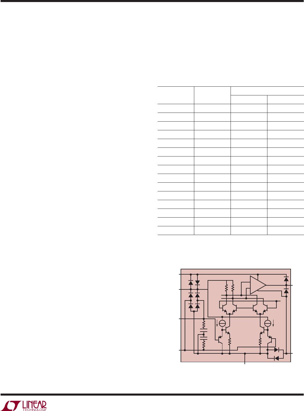
Figure 1. Simplifi ed Circuit Schematic
of the LTC5598 (Only I-Half is Drawn)
BBPI
BBMI
GND
LOMI LOPI
GNDRF
RF
FROM
Q
55682 F01
30Ω
30Ω
4pF
4pF
LTC5598
V
CC1
= 5V
V
CMBB
= 0.5V
DC
V
CC2
= 5V
BUFFER

LTC5598IUF#PBF

Mfr. #:
Manufacturer:
Analog Devices Inc.
Description:
Modulator / Demodulator 5MHz to 1600MHz Direct Quadrature Modulator
Lifecycle:
New from this manufacturer.
Delivery:
DHL FedEx Ups TNT EMS
Payment:
T/T Paypal Visa MoneyGram Western Union

Products related to this Datasheet