LTC5598
4
5598f
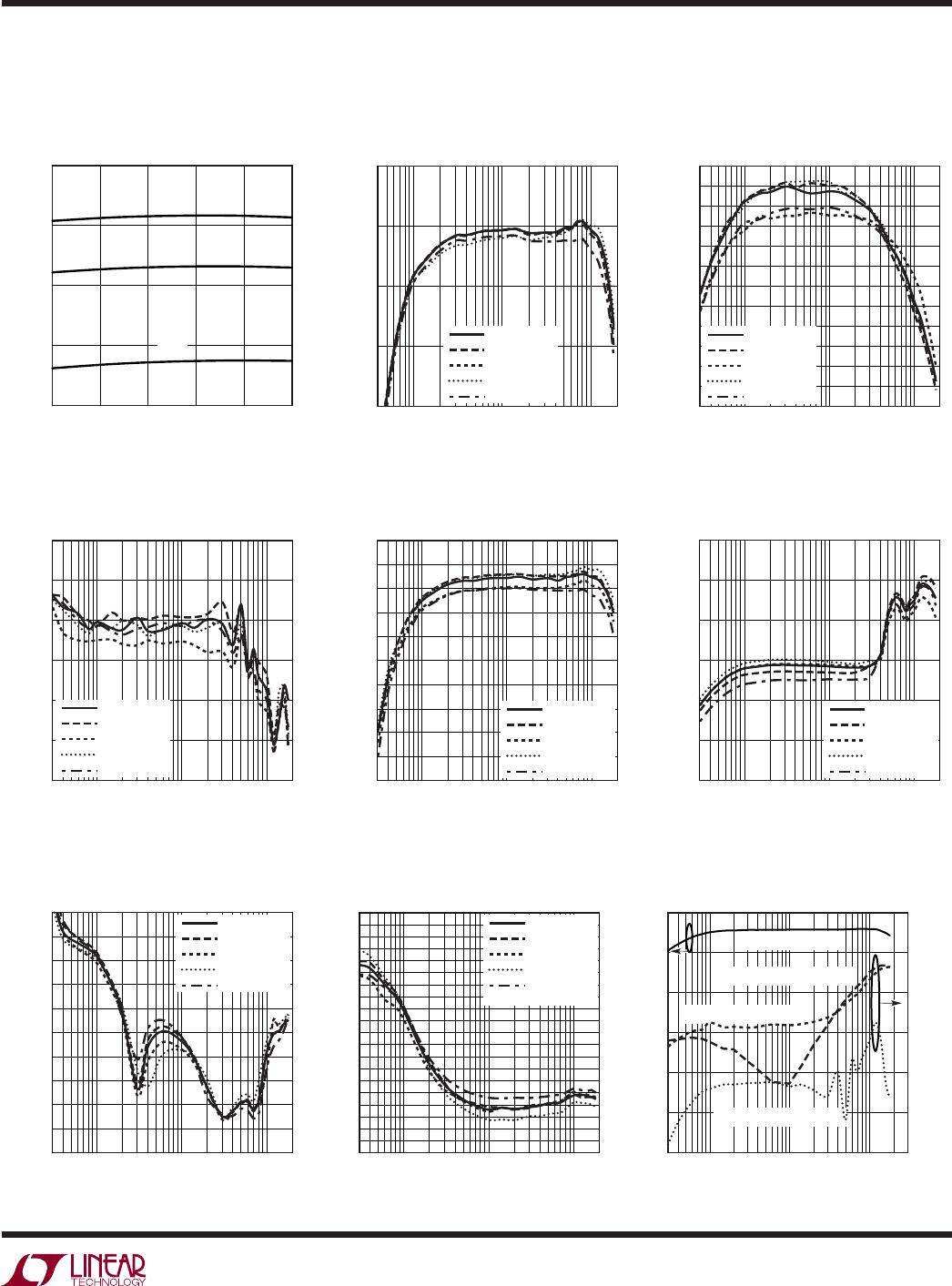
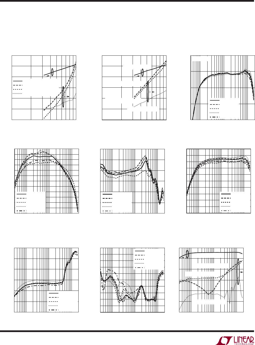
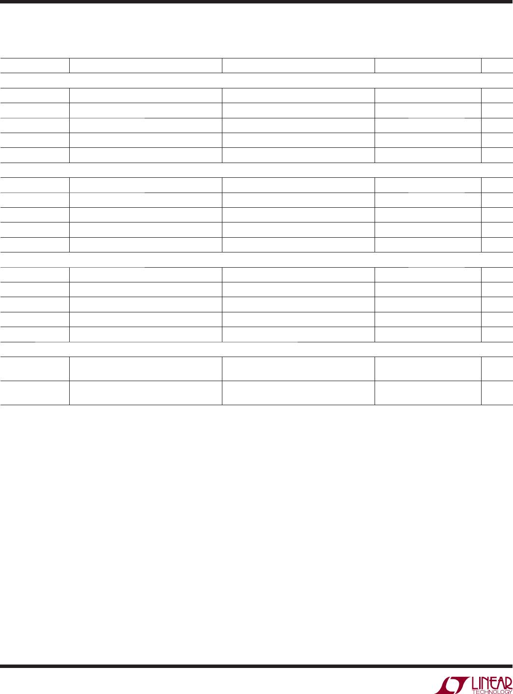
ELECTRICAL CHARACTERISTICS
V
CC
= 5V, EN = 5V, T
A
= 25ºC, P
LO
= 0dBm, single-ended; BBPI, BBMI,
BBPQ, BBMQ common-mode DC voltage V
CMBB
= 0.5V
DC
, I&Q baseband input signal = 100kHz CW, 0.8V
PP,DIFF
each, I&Q 90° shifted
(lower side-band selection), unless otherwise noted. (Note 11)
SYMBOL PARAMETER CONDITIONS MIN TYP MAX UNITS
LO INPUT (LOP)
f
LO
LO Frequency Range 5 to 1600 MHz
P
LO,DIFF
Differential LO Input Power Range –10 to 20 dBm
P
LO, SE
Single-Ended LO Input Power Range –10 to 12 dBm
S
11, ON
LO Input Return Loss EN = High –10.5 dB
S
11, OFF
LO Input Return Loss EN = Low –9.6 dB
BASEBAND INPUTS (BBPI, BBMI, BBPQ, BBMQ)
BW
BB
Baseband Bandwidth -3dB Bandwidth >400 MHz
I
b,BB
Baseband Input Current Single-Ended –68 μA
R
IN, SE
Input Resistance Single-Ended –7.4 kΩ
V
CMBB
DC Common-Mode Voltage Externally Applied 0.5 V
V
SWING
Amplitude Swing No Hard Clipping, Single-Ended 0.86 V
P-P
POWER SUPPLY (V
CC1
, V
CC2
)
V
CC
Supply Voltage 4.5 5 5.25 V
I
CC(ON)
Supply Current EN = High, I
CC1
+ I
CC2
130 165 200 mA
I
CC(OFF)
Supply Current, Sleep Mode EN = 0V, I
CC1
+ I
CC2
0.24 0.9 mA
t
ON
Turn-On Time EN = Low to High (Notes 8, 10) 75 ns
t
OFF
Turn-Off Time EN = High to Low (Notes 9, 10) 10 ns
POWER UP/DOWN
Enable Input High Voltage
Input High Current
EN = High
EN = 5V
2
43
V
μA
Sleep Input Low Voltage
Input Low Current
EN = Low
EN = 0V –40
1V
μA
Note 1: Stresses beyond those listed under Absolute Maximum Ratings
may cause permanent damage to the device. Exposure to any Absolute
Maximum Rating condition for extended periods may affect device
reliability and lifetime.
Note 2: The LTC5598 is guaranteed functional over the operating
temperature range –40ºC to 85ºC.
Note 3: At 6MHz offset from the LO signal frequency. 100nF between BBPI
and BBMI, 100nF between BBPQ and BBMQ.
Note 4: Baseband is driven by 2MHz and 2.1MHz tones with 1V
PP,DIFF
for
two-tone signals at each I or Q input (0.5V
PP,DIFF
for each tone).
Note 5: IM2 is measured at LO frequency – 4.1MHz.
Note 6: IM3 is measured at LO frequency – 1.9 MHz and LO frequency
– 2.2MHz.
Note 7: Amplitude average of the characterization data set without image
or LO feedthrough nulling (unadjusted).
Note 8: RF power is within 10% of fi nal value.
Note 9: RF power is at least 30dB lower than in the ON state.
Note 10: External coupling capacitors at pins LOP, LOM and RF are 100pF
each.
Note 11: Tests are performed as shown in the confi guration of Figure 10.
The LO power is applied to J3 while J5 is terminated with 50Ω to ground
for single-ended LO drive.