LTC2637
22
2637fb
OPERATION
Figure 3. Command and Data Input Format
C3
1ST DATA BYTE
Input Word (LTC2637-12)
Write Word Protocol for LTC2637
C2
C1
C0
A3
A2
A1
A1
D9D10D11
S
W ACK
SLAVE ADDRESS
1ST DATA BYTE
D8
D7 D6 D5 D4
D3
D2
D1 D0 X X X
X
ACK 2ND DATA BYTE ACK 3RD DATA BYTE ACK P
2637 F03
2ND DATA BYTE
INPUT WORD
3RD DATA BYTE
C3
1ST DATA BYTE
Input Word (LTC2637-10)
C2
C1
C0
A3
A2
A1
A0
D7D8D9
D6
D5 D4 D3 D2
D1
D0
XXXXX
X
2ND DATA BYTE 3RD DATA BYTE
C3
1ST DATA BYTE
Input Word (LTC2637-8)
C2
C1
C0
A3
A2
A1
A0
D5D6D7
D4
D3 D2 D1 D0
X
X
XXXXX
X
2ND DATA BYTE 3RD DATA BYTE
The LTC2637-LMI/ LTC2637-LMX/ LTC2637-LZ provides
a full-scale output of 2.5V. The LTC2637-HMI/ LTC2637-
HMX/ LTC2637-HZ provides a full-scale output of 4.096V.
The internal reference can be useful in applications where
the supply voltage is poorly regulated. Internal Reference
mode can be selected by using command 0110b, and is
the power-on default for LTC2637-HZ/ LTC2637-LZ, as
well as for LTC2637-HMI/ LTC2637-LMI.
The 10ppm/°C, 1.25V (LTC2637-LMI/ LTC2637-LMX/
LTC2637-LZ) or 2.048V (LTC2637-HMI/ LTC2637-HMX/
LTC2637-HZ) internal reference is available at the REF pin.
Adding bypass capacitance to the REF pin will improve
noise performance; and up to 10µF can be driven without
oscillation. The REF output must be buffered when driving
an external DC load current.
Alternatively, the DAC can operate in External Reference
mode using command 0111b. In this mode, an input voltage
supplied externally to the REF pin provides the reference
(1V ≤ V
REF
≤ V
CC
) and the supply current is reduced. The
external reference voltage supplied sets the full-scale DAC
output voltage. External Reference mode is the power-on
default for LTC2637-HMX/ LTC2637-LMX.
The reference mode of LTC2637-HZ/ LTC2637-LZ/ LTC2637-
HMI/ LTC2637-LMI (internal reference power-on default),
can be changed by software command after power up. The
same is true for LTC2637-HMX/ LTC2637-LMX (external
reference power-on default).
Power-Down Mode
For power-constrained applications, power-down mode can
be used to reduce the supply current whenever less than
eight DAC outputs are needed. When in power-down, the
buffer amplifi ers, bias circuits, and integrated reference
circuits are disabled, and draw essentially zero current.
The DAC outputs are put into a high-impedance state, and
the output pins are passively pulled to ground through in-
dividual 200k resistors. Input and DAC register contents
are not disturbed during power down.
Any DAC channel or combination of channels can be put
into power-down mode by using command 0100b in
combination with the appropriate DAC address, (n). The
supply current is reduced approximately 10% for each DAC
powered down. The integrated reference is automatically
powered down when external reference is selected using
LTC2637
23
2637fb
OPERATION
command 0111b. In addition, all the DAC channels and
the integrated reference together can be put into power-
down mode using Power Down Chip command 0101b.
When the integrated reference and all DAC channels are
in power-down mode, the REF pin becomes high imped-
ance (typically > 1G). For all power-down commands
the 16-bit data word is ignored.
Normal operation resumes after executing any command
that includes a DAC update, (as shown in Table 1). The
selected DAC is powered up as its voltage output is up-
dated. When a DAC which is in a powered-down state is
powered up and updated, normal settling is delayed. If
less than eight DACs are in a powered-down state prior
to the update command, the power-up delay time is 10µs.
However, if all eight DACs and the integrated reference
are powered down, then the main bias generation circuit
block has been automatically shut down in addition to
the DAC amplifi ers and reference buffers. In this case,
the power up delay time is 12µs. The power-up of the
integrated reference depends on the command that pow-
ered it down. If the reference is powered down using the
Select External Reference Command (0111b), then it can
only be powered back up using Select Internal Reference
Command (0110b). However, if the reference was powered
down using Power Down Chip Command (0101b), then in
addition to Select Internal Reference Command (0110b),
any command that powers up the DACs will also power
up the integrated reference.
Voltage Output
The LTC2637’s DAC output integrated rail-to-rail amplifi ers
have guaranteed load regulation when sourcing or sinking
up to 10mA at 5V, and 5mA at 3V.
Load regulation is a measure of the amplifi ers ability to
maintain the rated voltage accuracy over a wide range of
load current. The measured change in output voltage per
change in forced load current is expressed in LSB/mA.
DC output impedance is equivalent to load regulation, and
may be derived from it by simply calculating a change in
units from LSB/mA to ohms. The amplifi ers DC output
impedance is 0.1 when driving a load well away from
the rails.
When drawing a load current from either rail, the output
voltage headroom with respect to that rail is limited by
the 50 typical channel resistance of the output devices
(e.g., when sinking 1mA, the minimum output voltage is
50 • 1mA, or 50mV). See the graph “Headroom at Rails
vs. Output Current” in the Typical Performance Charac-
teristics section.
The amplifi er is stable driving capacitive loads of up to
500pF.
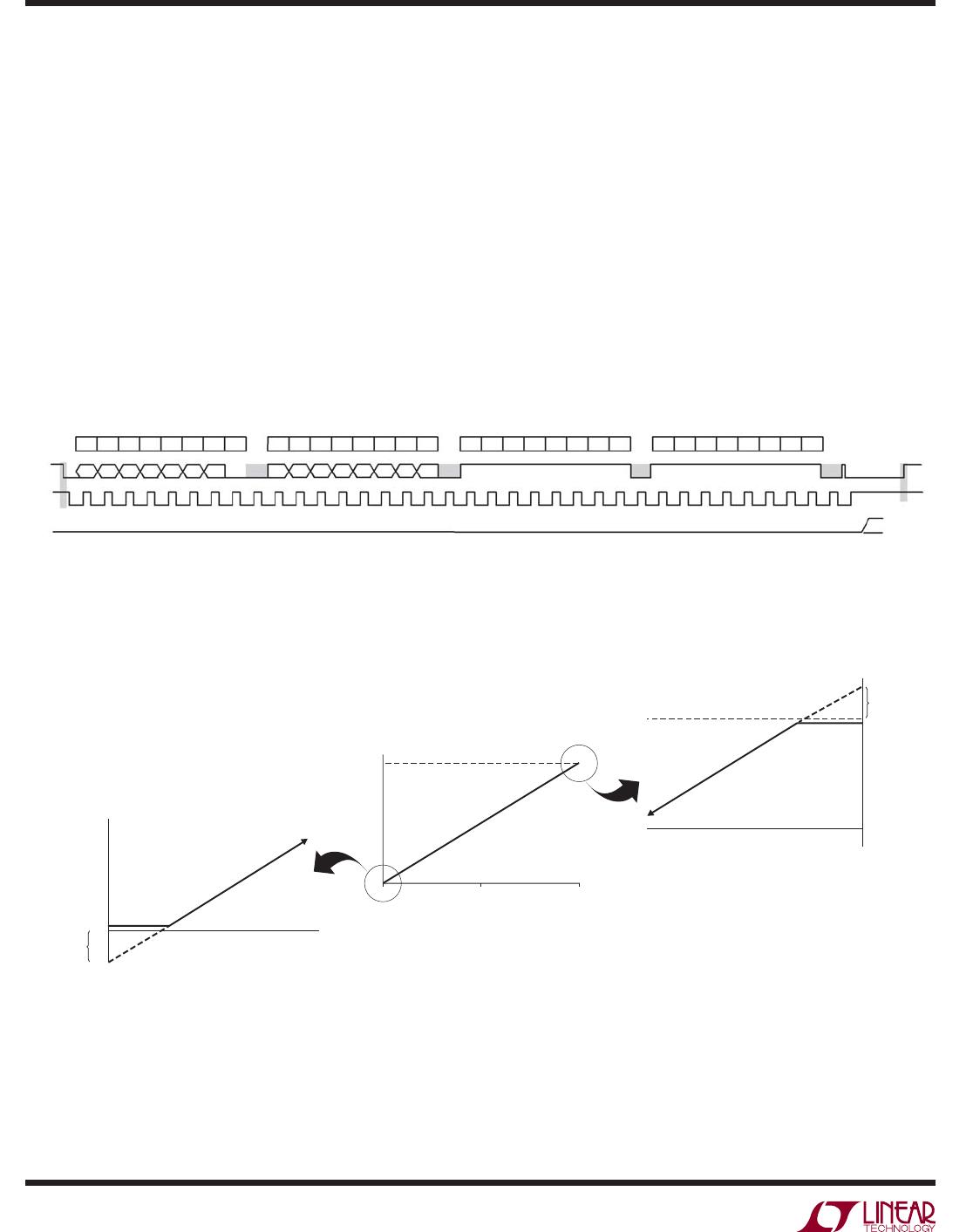
Rail-to-Rail Output Considerations
In any rail-to-rail voltage output device, the output is lim-
ited to voltages within the supply range.
Since the analog output of the DAC cannot go below ground,
it may limit for the lowest codes as shown in Figure 5b.
Similarly, limiting can occur near full scale when the REF
pin is tied to V
CC
. If V
REF
= V
CC
and the DAC full-scale error
(FSE) is positive, the output for the highest codes limits
at V
CC
, as shown in Figure 5c. No full-scale limiting can
occur if V
REF
is less than V
CC
–FSE.
Offset and linearity are defi ned and tested over the region
of the DAC transfer function where no output limiting can
occur.
Board Layout
The PC board should have separate areas for the analog and
digital sections of the circuit. A single, solid ground plane
should be used, with analog and digital signals carefully
routed over separate areas of the plane. This keeps digital
signals away from sensitive analog signals and minimizes
the interaction between digital ground currents and the
LTC2637
24
2637fb
analog section of the ground plane. The resistance from
the LTC2637 GND pin to the ground plane should be as
low as possible. Resistance here will add directly to the
effective DC output impedance of the device (typically
0.1). Note that the LTC2637 is no more susceptible to
this effect than any other parts of this type; on the con-
trary, it allows layout-based performance improvements
to shine rather than limiting attainable performance with
excessive internal resistance.
Another technique for minimizing errors is to use a sepa-
rate power ground return trace on another board layer.
The trace should run between the point where the power
supply is connected to the board and the DAC ground pin.
Thus the DAC ground pin becomes the common point for
analog ground, digital ground, and power ground. When
the LTC2637 is sinking large currents, this current fl ows
out the ground pin and directly to the power ground trace
without affecting the analog ground plane voltage.
It is sometimes necessary to interrupt the ground plane
to confi ne digital ground currents to the digital portion of
the plane. When doing this, make the gap in the plane only
as long as it needs to be to serve its purpose and ensure
that no traces cross over the gap.
OPERATION
A6 A5 A4 A3 A2 A1 A0 W C3
C3ACK
SLAVE ADDRESS
ACK ACK ACK
C2 C1 C0
A3 A2 A1 A0
D11 D10 D9 D8
D7 D6 D5 D4
D3 D2 D1 D0
XXXX
A6
START STOP
FULL-SCALE
VOLTAGE
ZERO-SCALE
VOLTAGE
SDA
SCL
X = DON’T CARE
V
OUT
A5 A4 A3 A2 A1 A0 C2 C1 C0 A3 A2 A1 A0
8912345
67
12345
67
8912345
67 89123456789
COMMAND/ADDRESS MS DATA LS DATA
2637 F04
Figure 4. Typical LTC2637 Input Waveform—Programming DAC Output for Full-Scale
Figure 5. Effects of Rail-to-Rail Operation On a DAC Transfer Curve (Shown for 12 Bits).
(a) Overall Transfer Function
(b) Effect of Negative Offset for Codes Near Zero
(c) Effect of Positive Full-Scale Error for Codes Near Full-Scale
2637 F04
INPUT CODE
(b)
OUTPUT
VOLTAGE
NEGATIVE
OFFSET
0V
0V
2,0480 4,095
INPUT CODE
OUTPUT
VOLTAGE
(a)
V
REF
= V
CC
V
REF
= V
CC
(c)
INPUT CODE
OUTPUT
VOLTAGE
POSITIVE
FSE

LTC2637HMS-HMX10#TRPBF

Mfr. #:
Manufacturer:
Analog Devices Inc.
Description:
Digital to Analog Converters - DAC 10-Bit I2C Octal DAC (4.096V ref, Reset to Mid-Scale, Ext. Ref)
Lifecycle:
New from this manufacturer.
Delivery:
DHL FedEx Ups TNT EMS
Payment:
T/T Paypal Visa MoneyGram Western Union