LTC2637
9
2637fb
ELECTRICAL CHARACTERISTICS
The l denotes the specifi cations which apply over the full operating
temperature range, otherwise specifi cations are at T
A
= 25°C. V
CC
= 4.5V to 5.5V, V
OUT
unloaded unless otherwise specifi ed.
LTC2637-HMI12/ LTC2637-HMI10/ LTC2637-HMI8/ LTC2637-HMX12/ LTC2637-HMX10/ LTC2637-HMX8/ LTC2637-HZ12/ LTC2637-HZ10/
LTC2637-HZ8 (V
FS
=4.096V)
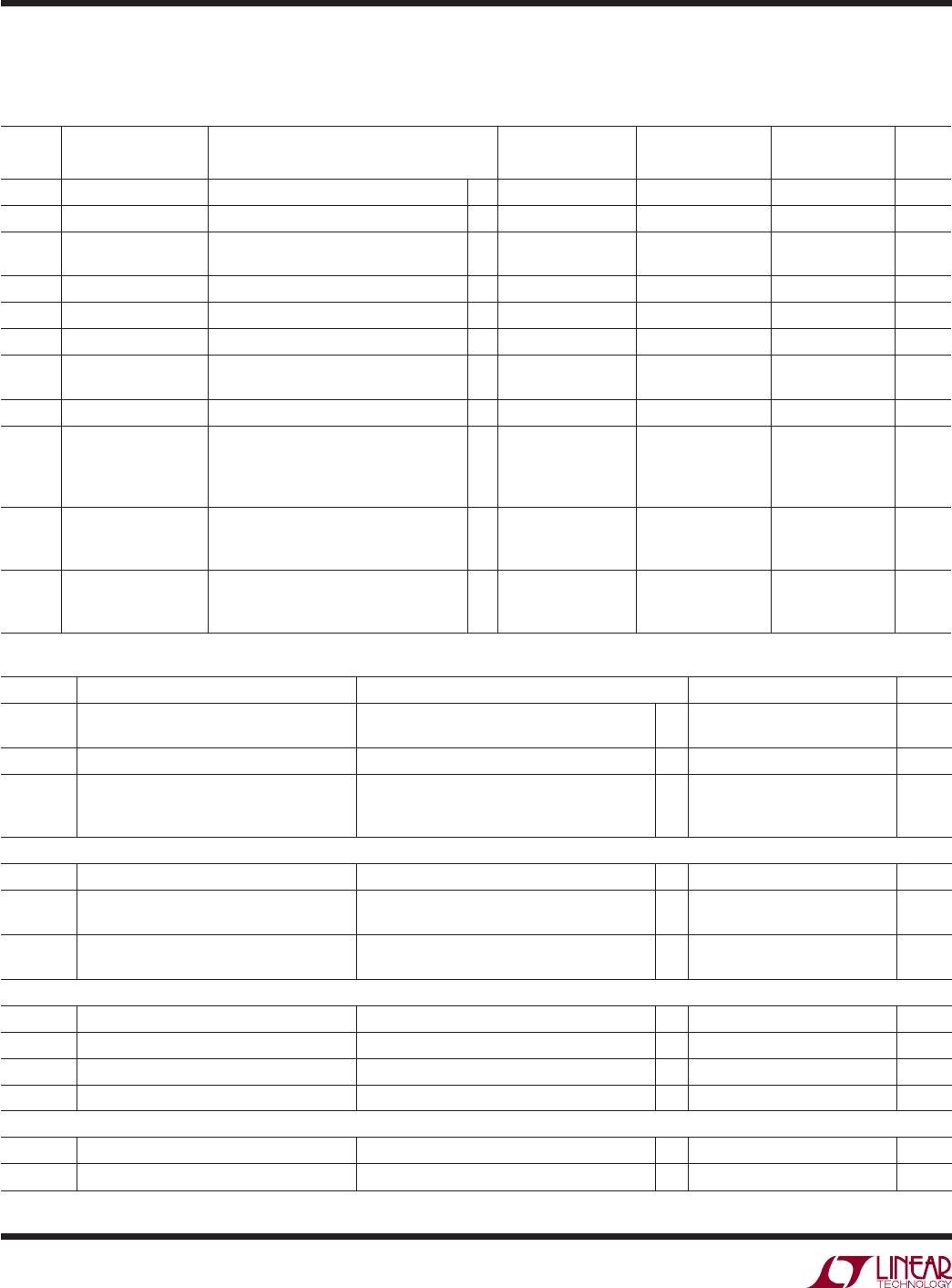
SYMBOL PARAMETER CONDITIONS MIN TYP MAX UNITS
Output Impedance 0.5 k
Capacitive Load Driving 10 µF
Short Circuit Current V
CC
= 5.5V; REF Shorted to GND 4 mA
Digital I/O
V
IL
Low Level Input Voltage (SDA and SCL) (Note 14)
l
–0.5 0.3V
CC
V
V
IH
High Level Input Voltage (SDA and SCL) (Note 11)
l
0.7V
CC
V
V
IL(CAn)
Low Level Input Voltage on CAn
(n = 0, 1, 2)
See Test Circuit 1
l
0.15V
CC
V
V
IH(CAn)
High Level Input Voltage on CAn
(n = 0, 1, 2)
See Test Circuit 1
l
0.85V
CC
V
R
INH
Resistance from CAn (n=0, 1,2)
to V
CC
to Set CAn = V
CC
See Test Circuit 2
l
10 k
R
INL
Resistance from CAn (n=0, 1,2)
to GND to Set CAn = GND
See Test Circuit 2
l
10 k
R
INF
Resistance from CAn (n=0, 1,2)
to V
CC
or GND to Set CAn = Float
See Test Circuit 2
l
2M
V
OL
Low Level Output Voltage Sink Current = 3mA
l
0 0.4 V
t
OF
Output Fall Time V
O
= V
IH(MIN)
to V
O
= V
IL(MAX)
,
C
B
= 10pF to 400pF (Note 12)
l
20 + 0.1C
B
250 ns
t
SP
Pulse Width of Spikes Suppressed
by Input Filter
l
050ns
I
IN
Input Leakage 0.1V
CC
≤ V
IN
≤ 0.9V
CC
l
±1 µA
C
IN
I/O Pin Capacitance (Note 8)
l
10 pF
C
B
Capacitive Load for Each Bus Line
l
400 pF
C
CAn
External Capacitive Load on Address
Pin CAn (n=0, 1,2)
l
10 pF
AC Performance
t
S
Settling Time V
CC
= 3V (Note 9)
±0.39% (±1LSB at 8 Bits)
±0.098% (±1LSB at 10 Bits)
±0.024% (±1LSB at 12 Bits)
3.9
4.3
5
µs
µs
µs
Voltage Output Slew Rate 1 V/µs
Capacitive Load Driving 500 pF
Glitch Impulse At Mid-Scale Transition 3 nV•s
DAC-to-DAC Crosstalk 1 DAC held at FS, 1 DAC Switched 0 to FS 3 nV•s
Multiplying Bandwidth External Reference 320 kHz
e
n
Output Voltage Noise Density At f = 1kHz, External Reference
At f = 10kHz, External Reference
At f = 1kHz, Internal Reference
At f = 10kHz, Internal Reference
180
160
250
230
nV/√Hz
nV/√Hz
nV/√Hz
nV/√Hz
Output Voltage Noise 0.1Hz to 10Hz, External Reference
0.1Hz to 10Hz, Internal Reference
0.1Hz to 200kHz, External Reference
0.1Hz to 200kHz, Internal Reference
35
50
680
750
µV
P-P
µV
P-P
µV
P-P
µV
P-P