LTC4440
1
4440fb
For more information www.linear.com/LTC4440
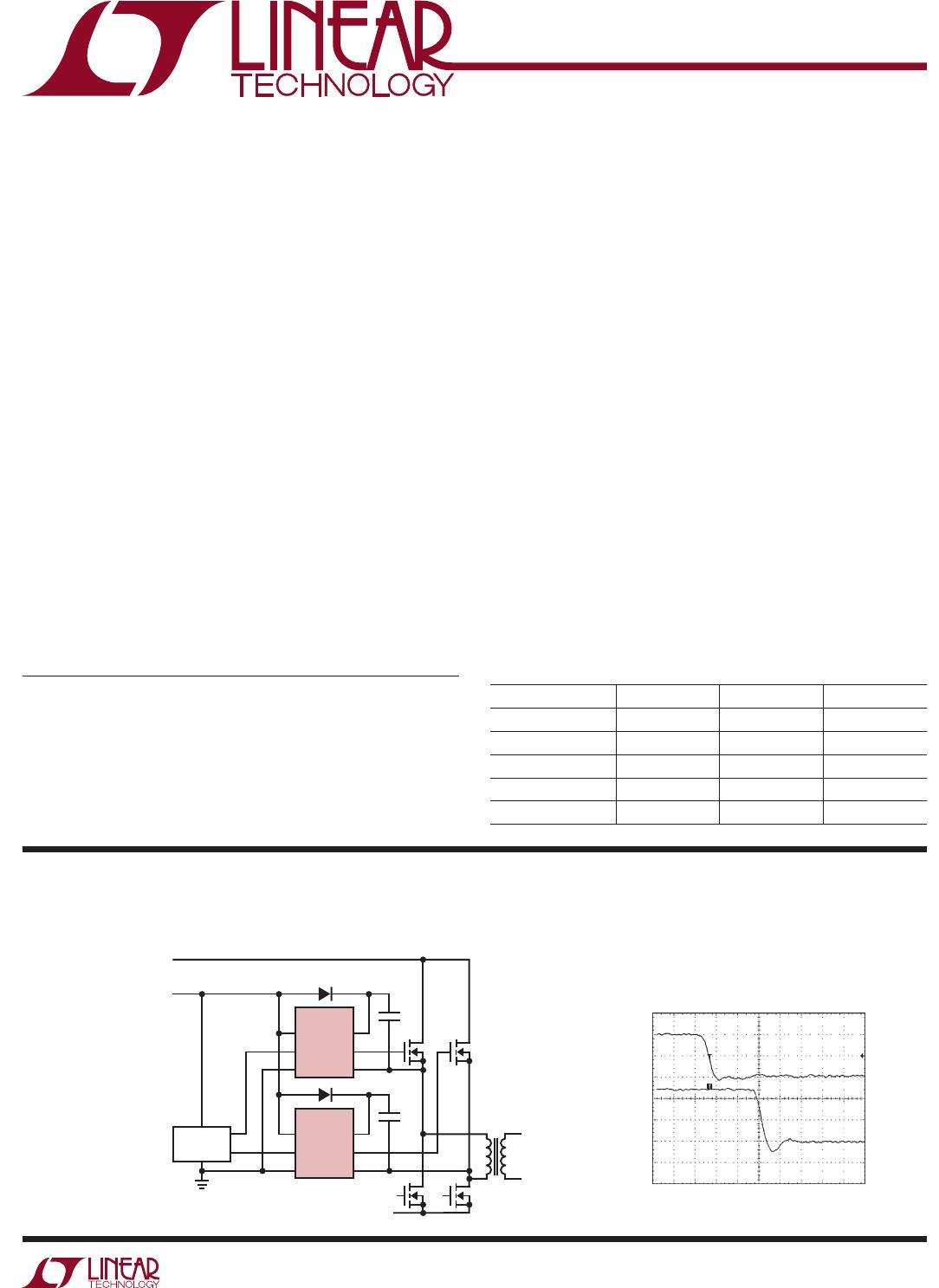
TYPICAL APPLICATION
Synchronous Phase-Modulated Full-Bridge Converter
LTC4440 Driving a 1000pF
Capacitive Load
V
CC
INP
GND
BOOST
TG
TS
LTC4440
IN
36V TO 72V
(ABS MAX)
V
CC
8V TO 15V
V
CC
INP
GND
BOOST
TG
TS
LTC4440
V
CC
LTC3722-1
• •
INPUT
(INP)
2V/DIV
OUTPUT
5V/DIV
FEATURES DESCRIPTION
High Speed, High Voltage
High Side Gate Driver
The LT C
®
4440 is a high frequency high side N-channel
MOSFET gate driver that is designed to operate in ap-
plications with
V
IN
voltages up to 80V. The LTC4440 can
also withstand and continue to function during 100V V
IN
transients. The powerful driver capability reduces switch-
ing losses
in MOSFETs with high gate capacitances. The
LTC4440’s
pull-up has a peak output current of 2.4A and
its pull-down has an output impedance of 1.5Ω.
The LTC4440 features supply independent TTL/CMOS
compatible input thresholds with 350mV of hysteresis.
The input logic signal is internally level-shifted to the
bootstrapped supply, which may function at up to 115V
above ground.
The LTC4440 contains both high side and low side under
-
voltage lockout circuits that disable the external MOSFET
when activated.
The LTC4440 is available in the low profile (1mm) SOT-23
and thermally enhanced 8-lead MSOP packages.
PARAMETER LTC4440 LTC4440-5 LTC4440A-5
Max Operating TS 80V 60V 80V
Absolute Max TS 100V 80V 100V
MOSFET Gate Drive 8V to 15V 4V to 15V 4V to 15V
V
CC
UV
+
6.3V 3.2V 3.2V
V
CC
UV
–
6.0V 3.04V 3.04V
APPLICATIONS
n
Wide Operating V
IN
Range: Up to 80V
n
Rugged Architecture Tolerant of 100V V
IN
Transients
n
Powerful 1.5Ω Driver Pull-Down
n
Powerful 2.4A Peak Current Driver Pull-Up
n
7ns Fall Time Driving 1000pF Load
n
10ns Rise Time Driving 1000pF Load
n
Drives Standard Threshold MOSFETs
n
TTL/CMOS Compatible Inputs with Hysteresis
n
Input Thresholds are Independent of Supply
n
Undervoltage Lockout
n
Low Profile (1mm) SOT-23 (ThinSOT)™ and
Thermally Enhanced 8-Pin MSOP Packages
n
Telecommunications Power Systems
n
Distributed Power Architectures
n
Server Power Supplies
n
High Density Power Modules
L, LT , LT C , LTM , Linear Technology and the Linear logo are registered trademarks and
ThinSOT is a trademark of Linear Technology Corporation. All other trademarks are the property
of their respective owners. Protected by U.S. Patents, including 6677210.