LTC4440
8
4440fb
For more information www.linear.com/LTC4440
APPLICATIONS INFORMATION
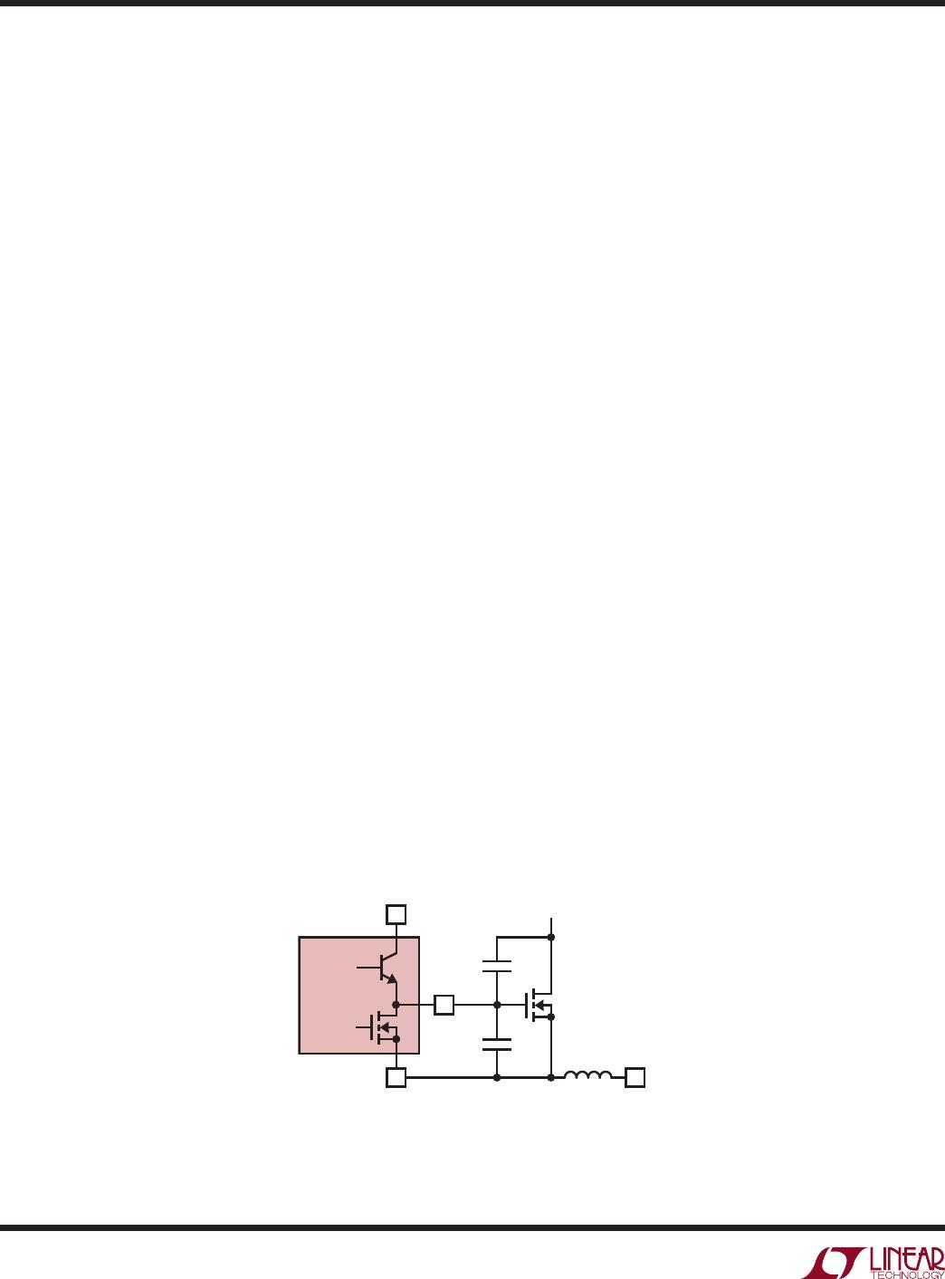
Figure 3. Capacitance Seen by TG During Switching
Overview
The LTC4440 receives a ground-referenced, low voltage
digital input signal to drive a high side N-channel power
MOSFET whose drain can float up to 100V above ground,
eliminating the need for a transformer between the low
voltage control signal and the high side gate driver. The
LTC4440 normally operates in applications with input
supply voltages (V
IN
) up to 80V, but is able to withstand
and continue to function during 100V, 100ms transients
on the input supply.
The powerful output driver of the LTC4440 reduces the
switching losses of the power MOSFET, which increase
with transition time. The LTC4440 is capable of driving a
1nF load with 10ns rise and 7ns fall times using a boot
-
strapped supply voltage V
BOOST–TS
of 12V.
Input Stage
The LTC4440 employs TTL/CMOS compatible input thresh
-
olds that allow a low voltage digital signal to drive standard
power MOSFETs. The LTC4440 contains an internal voltage
regulator that biases the input buffer, allowing the input
thresholds (V
IH
= 1.6V, V
IL
= 1.25V) to be independent of
variations in V
CC
. The 350mV hysteresis between V
IH
and
V
IL
eliminates false triggering due to noise during switching
transitions. However, care should be taken to keep this
pin from any noise pickup, especially in high frequency,
high voltage applications. The LTC4440 input buffer has a
high input impedance and draws negligible input current,
simplifying the drive circuitry required for the input.
Output Stage
A simplified version of the LTC4440’s output stage is
shown in Figure 3 . The pull-down device is an N-channel
MOSFET (N1) and the pull-up device is an NPN bipolar
junction transistor (Q1). The output swings from the lower
rail (TS) to within an NPN V
BE
(~0.7V) of the positive rail
(BOOST). This large voltage swing is important in driv-
ing external
power MOSFETs, whose R
DS(ON)
is inversely
proportional to its gate overdrive voltage (V
GS
– V
TH
).
The LTC4440’s peak pull-up (Q1) current is 2.4A while the
pull-down (N1) resistance is 1.5Ω. The low impedance
of N1 is required to discharge the power MOSFET’s gate
capacitance during high-to-low signal transitions. When the
power MOSFET’s gate is pulled low (gate shorted to source
through N1) by the LTC4440, its source (TS) is pulled low
by its load (e.g.,
an inductor or resistor). The slew rate
of
the source/gate voltage causes current to flow back to
the MOSFET’s gate through the gate-to-drain capacitance
(C
GD
). If the MOSFET driver does not have sufficient sink
current capability (low output impedance), the current
through the power MOSFET’s C
GD
can momentarily pull
the gate high, turning the MOSFET back on.
A similar scenario exists when the LTC4440 is used to drive
a low side MOSFET. When the low side power MOSFET’s
gate is pulled low by the LTC4440, its drain voltage is
pulled high by its load (e.g., inductor or resistor). The slew
rate of the drain voltage causes current to flow back to the
MOSFET’s gate through its gate-to-drain capacitance. If
IN
UP TO 100V
V
–
TG
C
GD
POWER
MOSFET
LOAD
INDUCTOR
C
GS
4440 F03
LTC4440
Q1
N1