8Mb
SMART 3 BOOT BLOCK FLASH MEMORY
09005aef81136a91 Micron Technology, Inc., reserves the right to change products or specifications without notice.
Q10.fm - Rev. E 6/04 EN
22 ©2001 Micron Technology, Inc. All rights reserved.
Figure 11: Byte-Wide READ Cycle
1
Timing Parameters
Commercial Temperature (0°C T
A
+70°C)
Extended Temperature (-40°C T
A
+85°C)
NOTE:
1. BYTE# = LOW (MT28F800B3 only).
VALID DATA
VALID ADDRESS
CE#
A0–A18/(A19)
OE#
DQ0–DQ7
DON’T CARE
UNDEFINED
t
RC
t
ACE
t
AOE
t
OD
t
OH
t
AA
WE#
RP#
V
IH
V
IL
V
IH
V
IL
V
IH
V
IL
V
IH
V
IL
V
IH
V
IL
V
IH
V
IL
t
RWH
DQ8–DQ14
V
IH
V
IL
HIGH-Z
SYMBOL
-9/-9 ET
UNITSMIN MAX
t
RC
90 ns
t
ACE
90 ns
t
AOE
40 ns
t
AA
90 ns
t
RWH
1,000 ns
t
OD
25 ns
t
OH
0ns
SYMBOL
-9/-9 ET
UNITSMIN MAX
8Mb
SMART 3 BOOT BLOCK FLASH MEMORY
09005aef81136a91 Micron Technology, Inc., reserves the right to change products or specifications without notice.
Q10.fm - Rev. E 6/04 EN
23 ©2001 Micron Technology, Inc. All rights reserved.
NOTE:
1. WRITE operations are tested at VPP voltages equal to or less than the previous ERASE.
2. Absolute WRITE/ERASE protection when VPP VPPLK.
3. When 3.3V Vcc and VPP are used, Vcc cannot exceed VPP by more than 500mV during WRITE and ERASE operations.
4. All currents are in RMS unless otherwise noted.
5. Applies to MT28F800B3 only.
6. Applies to MT28F008B3 and MT28F800B3 with BYTE# = LOW.
7. Parameter is specified when device is not accessed. Actual current draw will be I
CC10 plus read current if a READ is
executed while the device is in erase suspend mode.
Table 13: Recommended DC WRITE/ERASE Conditions
1
Commercial Temperature (0°C T
A
+70°C) and Extended Temperature (-40°C T
A
+85°C); Vcc = +3.3V ±0.3V
PARAMETER/CONDITION SYMBOL MIN MAX UNITS NOTES
V
PP WRITE/ERASE lockout voltage
V
PPLK –1.5V 2
V
PP voltage during WRITE/ERASE operation
V
PPH13.0 3.6 V 3
V
PP voltage during WRITE/ERASE operation
V
PPH24.5 5.5 V
Boot block unlock voltage
V
HH 10 12.6 V
Vcc WRITE/ERASE lockout voltage
V
LKO 2–V
Table 14: WRITE/ERASE Current Drain
4
Commercial Temperature (0°C T
A
+70°C) and Extended Temperature (-40°C T
A
+85°C); Vcc = +3.3V ±0.3V
PARAMETER/CONDITION SYMBOL
3.3V VPP 5V VPP
UNITS NOTESMAX MAX
WORD WRITE CURRENT: Vcc SUPPLY
I
CC720 20mA 5
WORD WRITE CURRENT: V
PP SUPPLY
I
PP320 20mA 5
BYTE WRITE CURRENT: Vcc SUPPLY
I
CC820 20mA 6
BYTE WRITE CURRENT: V
PP SUPPLY
I
PP420 20mA 6
ERASE CURRENT: Vcc SUPPLY
I
CC925 25mA
ERASE CURRENT: V
PP SUPPLY
I
PP525 30mA
ERASE SUSPEND CURRENT: Vcc SUPPLY
(ERASE suspended)
I
CC10 8 10 mA 7
ERASE SUSPEND CURRENT: V
PP SUPPLY
(ERASE suspended)
IPP6200200 µA
8Mb
SMART 3 BOOT BLOCK FLASH MEMORY
09005aef81136a91 Micron Technology, Inc., reserves the right to change products or specifications without notice.
Q10.fm - Rev. E 6/04 EN
24 ©2001 Micron Technology, Inc. All rights reserved.
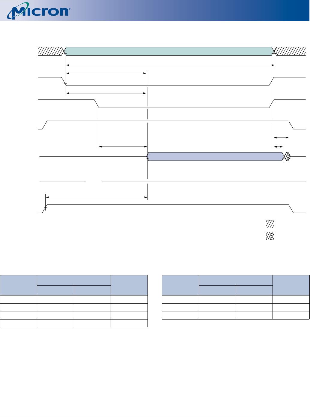
NOTE:
1. Measured with VPP = VPPH1 = 3.3V.
2. Measured with VPP = VPPH2 = 5V.
3. RP# should be held at V
HH or WP# held HIGH until boot block WRITE or ERASE is complete.
4. Polling status register before tWB is met may falsely indicate WRITE or ERASE completion.
5. WRITE/ERASE times are measured to valid status register data (SR7 = 1).
6. tREL is required to relock boot block after WRITE or ERASE to boot block.
7. Typical values measured at T
A
= +25ºC.
8. Assumes no system overhead.
9. Typical WRITE times use checkerboard data pattern.
Table 15: Speed-Dependent WRITE/ERASE AC Timing Characteristics and
Recommended AC Operating Conditions: WE# (CE#)-Controlled WRITEs
Commercial Temperature (0°C T
A
+70°C) and Extended Temperature (-40°C T
A
+85°C); Vcc = +3.3V ±0.3V
ACCHARACTERISTICS
SYMBOL
-9/-9 ET
UNITS NOTESPARAMETER MIN MAX
WRITE cycle time
t
WC
90 ns
WE# (CE#) HIGH pulse width
t
WPH (
t
CPH)
20 ns
WE# (CE#) pulse width
t
WP (
t
CP)
50 ns
Address setup time to WE# (CE#) HIGH
t
AS
50 ns
Address hold time from WE# (CE#) HIGH
t
AH
0ns
Data setup time to WE# (CE#) HIGH
t
DS
50 ns
Data hold time from WE# (CE#) HIGH
t
DH
0ns
CE# (WE#) setup time to WE# (CE#) LOW
t
CS (
t
WS)
0ns
CE# (WE#) hold time from WE# (CE#) HIGH
t
CH (
t
WH)
0ns
V
PP setup time to WE# (CE#) HIGH
t
VPS1
200 ns 1
V
PP setup time to WE# (CE#) HIGH
t
VPS2
100 ns 2
RP# HIGH to WE# (CE#) LOW delay
t
RS
1,000 ns
RP# at V
HH or WP# HIGH setup time to WE# (CE#) HIGH
t
RHS
100 ns 3
WRITE duration (WORD or BYTE WRITE)
t
WED1
s5
Boot BLOCK ERASE duration
t
WED2
100 ms 5
Parameter BLOCK ERASE duration
t
WED3
100 ms 5
Main BLOCK ERASE duration
t
WED4
500 ms 5
WE# (CE#) HIGH to busy status (SR7 = 0)
t
WB
200 ns 4
V
PP hold time from status data valid
t
VPH
0ns5
RP# at V
HH or WP# HIGH hold time from status data valid
t
RHH
0ns3
Boot block relock delay time
t
REL
100 ns 6
Table 16: Word/Byte WRITE and ERASE Duration Characteristics
PARAMETER
3.3V VPP 5V VPP
UNITS NOTESTYP MAX TYP MAX
Boot/parameter BLOCK ERASE time
0.5 7 0.4 7 s 7
Main BLOCK ERASE time
2.8141.514 s 7
Main BLOCK WRITE time (byte mode)
1.5 1 s 7, 8, 9
Main BLOCK WRITE time (word mode)
1.5 1 s 7, 8, 9

MT28F008B3VP-9 B TR

Mfr. #:
Manufacturer:
Micron
Description:
IC FLASH 8M PARALLEL 40TSOP I
Lifecycle:
New from this manufacturer.
Delivery:
DHL FedEx Ups TNT EMS
Payment:
T/T Paypal Visa MoneyGram Western Union