© Semiconductor Components Industries, LLC, 2013
April, 2013 − Rev. 26
1 Publication Order Number:
LM2931/D
LM2931, NCV2931 Series
100 mA, Adjustable Output,
LDO Voltage Regulator with
60 V Load Dump Protection
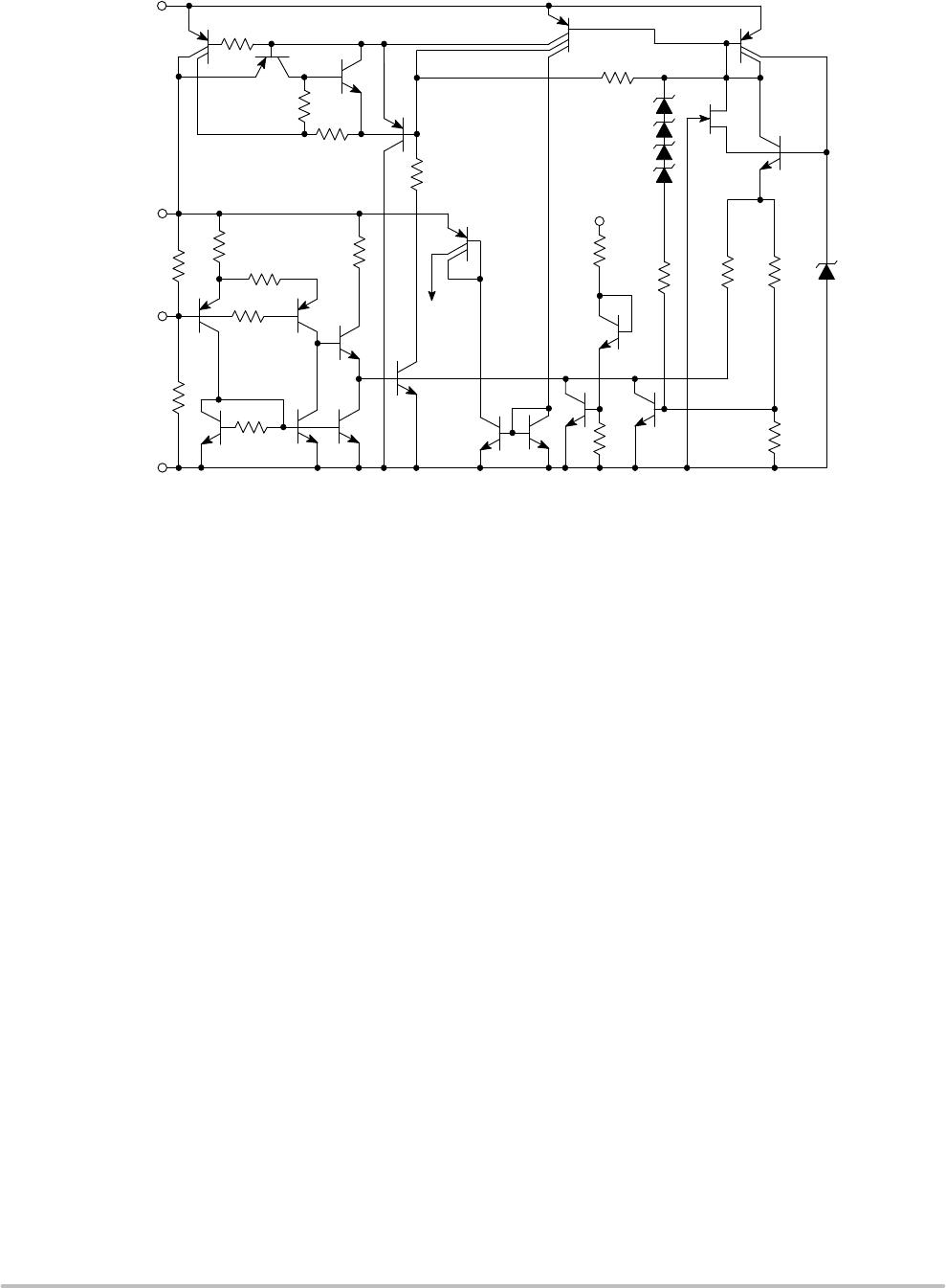
The LM2931 series consists of positive fixed and adjustable output
voltage regulators that are specifically designed to maintain proper
regulation with an extremely low input−to−output voltage differential.
These devices are capable of supplying output currents in excess of
100 mA and feature a low bias current of 0.4 mA at 10 mA output.
Designed primarily to survive in the harsh automotive environment,
these devices will protect all external load circuitry from input fault
conditions caused by reverse battery connection, two battery jump
starts, and excessive line transients during load dump. This series also
includes internal current limiting, thermal shutdown, and additionally,
is able to withstand temporary power−up with mirror−image insertion.
Due to the low dropout voltage and bias current specifications, the
LM2931 series is ideally suited for battery powered industrial and
consumer equipment where an extension of useful battery life is
desirable. The ‘C’ suffix adjustable output regulators feature an output
inhibit pin which is extremely useful in microprocessor−based systems.
Features
• Input−to−Output Voltage Differential of < 0.6 V @ 100 mA
• Output Current in Excess of 100 mA
• Low Bias Current
• 60 V Load Dump Protection
• −50 V Reverse Transient Protection
• Internal Current Limiting with Thermal Shutdown
• Temporary Mirror−Image Protection
• Ideally Suited for Battery Powered Equipment
• Economical 5−Lead TO−220 Package with Two Optional Leadforms
• Available in Surface Mount SOP−8, D
2
PAK and DPAK Packages
• High Accuracy (±2.5%) Reference (LM2931AC) Available
• NCV Prefix for Automotive and Other Applications Requiring
Unique Site and Control Change Requirements; AEC−Q100
Qualified and PPAP Capable
• Pb−Free Packages are Available
Applications
• Battery Powered Consumer Products
• Hand−held Instruments
• Camcorders and Cameras
FIXED
(Top View)
N.C.
GND
Input
N.C.
GND
Output18
54
ADJUSTABLE
(Top View)
Output
Inhibit
GND
Input
Adjust
GND
Output18
54
SOIC−8
D SUFFIX
CASE 751
1
8
TO−92
Z SUFFIX
CASE 29
FIXED OUTPUT VOLTAGE
Pin 1. Output
2. Ground
3. Input
TO−220
T SUFFIX
CASE 221AB
Pin 1. Input
2. Ground
3. Output
DPAK
DT SUFFIX
CASE 369C
D
2
PAK
D2T SUFFIX
CASE 936
TO−220
TH SUFFIX
CASE 314A
ADJUSTABLE OUTPUT VOLTAGE
Pin 1. Adjust
2. Output
Inhibit
3. Ground
4. Input
5. Output
TO−220
TV SUFFIX
CASE 314B
TO−220
T SUFFIX
CASE 314D
D
2
PAK
D2T SUFFIX
CASE 936A
See detailed ordering and shipping information in the package
dimensions section on page 12 of this data sheet.
ORDERING INFORMATION
See general marking and heatsink information in the device
marking section on page 15 of this data sheet.
DEVICE MARKING INFORMATION
1
2
3
1
3
1
3
1
5
1
1
5
1
5
1
5
http://onsemi.com
1
3
SOT−223
ST SUFFIX
CASE 318H
1
2
3
1