LM2931, NCV2931 Series
http://onsemi.com
8
, REFERENCE VOLTAGE (V)
ref
V
O
, OUTPUT VOLTAGE (V)
1.160
1.180
1.200
1.220
1.240
0 3.0 6.0 9.0 12 15 18 21 24
V
18.5
14
t, TIME (10 ms/DIV)
V
out
= 5.0 V
R
L
= 500 W
C
O
= 100 mF
C
O(ESR)
= 0.3 W
T
A
= 25°C
100
0
t, TIME (10 ms/DIV)
V
O
, OUTPUT VOLTAGE (V)
V
th(on/off)
, OUTPUT INHIBIT‐THRESHOLDS (V)
2.0
2.1
2.2
0 3.0 6.0 9.0 12 15 18 21 24
Output “On"
Output “Off"
2.4
2.5
2.6
2.3
LM2931C Adjustable
I
O
= 10 mA
V
in
= V
out
+ 1.0 V
T
A
= 25°C
V
in
= 14 V
V
out
= 5.0 V
C
in
= 1000 mF
C
O
= 100 mF
C
O(ESR)
= 0.3 W
T
A
= 25°C
LM2931C Adjustable
I
O
= 10 mA
V
in
= V
out
+ 1.0 V
T
A
= 25°C
OUTPUT CURRENT,
I (mA)
out
Δ
OUTPUT VOLTAGE DEVIATION,
O
, (2.0 mV/DIV)V
INPUT VOLTAGE,
V , (V)
in
Δ
OUTPUT VOLTAGE DEVIATION,
O
, (2.0 mV/DIV)V
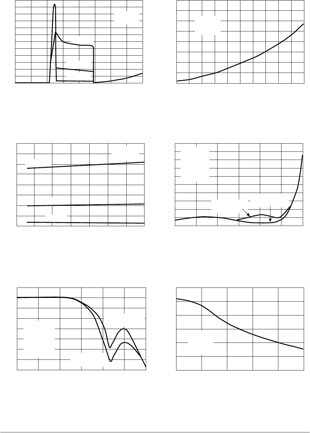
Figure 13. Line Regulation
Figure 14. Load Regulation
Figure 15. Reference Voltage versus Output Voltage Figure 16. Output Inhibit−Thresholds
versus Output Voltage
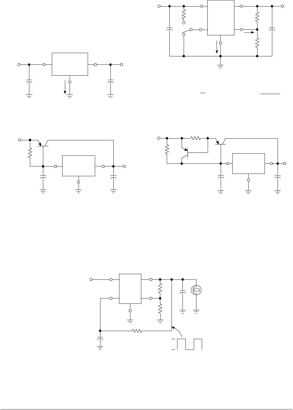
APPLICATIONS INFORMATION
The LM2931 series regulators are designed with many
protection features making them essentially blow−out
proof. These features include internal current limiting,
thermal shutdown, overvoltage and reverse polarity input
protection, and the capability to withstand temporary
power−up with mirror−image insertion. Typical application
circuits for the fixed and adjustable output device are shown
in Figures 17 and 18.
The input bypass capacitor C
in
is recommended if the
regulator is located an appreciable distance (≥ 4″) from the
supply input filter. This will reduce the circuit’s sensitivity
to the input line impedance at high frequencies.
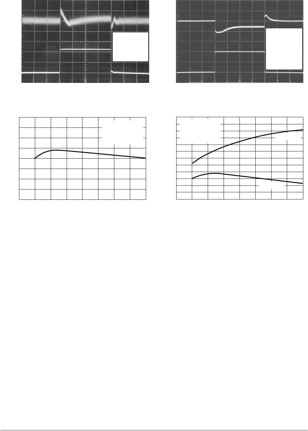
This regulator series is not internally compensated and
thus requires an external output capacitor for stability. The
capacitance value required is dependent upon the load
current, output voltage for the adjustable regulator, and the
type of capacitor selected. The least stable condition is
encountered at maximum load current and minimum output
voltage. Figure 22 shows that for operation in the “Stable”
region, under the conditions specified, the magnitude of the
output capacitor impedance |Z
O
| must not exceed 0.4 W. This
limit must be observed over the entire operating temperature
range of the regulator circuit.
With economical electrolytic capacitors, cold temperature
operation can pose a serious stability problem. As the
electrolyte freezes, around −30°C, the capacitance will
decrease and the equivalent series resistance (ESR) will
increase drastically, causing the circuit to oscillate. Quality
electrolytic capacitors with extended temperature ranges of
−40° to +85°C and −55° to +105°C are readily available.
Solid tantalum capacitors may be a better choice if small size
is a requirement, however, the maximum ⏐Z
O
⏐ limit over
temperature must be observed.
Note that in the stable region, the output noise voltage is
linearly proportional to ⏐Z
O
⏐
.
In effect, C
O
dictates the high
frequency roll−off point of the circuit. Operation in the area
titled “Marginally Stable” will cause the output of the
regulator to exhibit random bursts of oscillation that decay
in an under−damped fashion. Continuous oscillation occurs
when operating in the area titled “Unstable”. It is suggested
that oven testing of the entire circuit be performed with
maximum load, minimum input voltage, and minimum
ambient temperature.