LTC1863/LTC1867
1
18637fc
For more information www.linear.com/LTC1863
BLOCK DIAGRAM
DESCRIPTION
12-/16-Bit, 8-Channel
200ksps ADCs
FEATURES
APPLICATIONS
n
Industrial Process Control
n
High Speed Data Acquisition
n
Battery Operated Systems
n
Multiplexed Data Acquisition Systems
n
Imaging Systems
n
Sample Rate: 200ksps
n
16-Bit No Missing Codes and ±2LSB Max INL
n
8-Channel Multiplexer with:
n
Single Ended or Differential Inputs and
n
Unipolar or Bipolar Conversion Modes
n
SPI/MICROWIRE Serial I/O
n
Signal-to-Noise Ratio: 89dB
n
Single 5V Operation
n
On-Chip or External Reference
n
Low Power: 1.3mA at 200ksps, 0.76mA at 100ksps
n
Sleep Mode
n
Automatic Nap Mode Between Conversions
n
16-Pin Narrow SSOP Package
The LT C
®
1863/LTC1867 are pin-compatible, 8-channel
12-/16-bit A/D converters with serial I/O, and an internal
reference. The ADCs typically draw only 1.3mA from a
single 5V supply.
The 8-channel input multiplexer can be configured for
either single-ended or differential inputs and unipolar
or bipolar conversions (or combinations thereof). The
automatic nap and sleep modes benefit power sensitive
applications.
The
LTC1867’s DC performance is outstanding with a
±2LSB INL specification and no missing codes over tem-
perature. The signal-to-noise ratio (SNR) for the LTC1867
is typically 89dB, with the internal reference.
Housed in a compact, narrow 16-pin SSOP package, the
LTC1863/LTC1867 can be used in space-sensitive as well
as low-power applications.
CH0
CH1
CH2
CH3
CH4
CH5
CH6
CH7/COM
1
2
3
4
5
6
7
8
16
15
14
13
12
11
10
V
DD
GND
SDI
SDO
SCK
CS/CONV
V
REF
18637 BD
12-/16-BIT
200ksps
ADC
+
SERIAL
PORT
ANALOG
INPUT
MUX
REFCOMP
9
INTERNAL
2.5V REF
LTC1863/LTC1867
OUTPUT CODE
0
INL (LSB)
49152
18637 GO1
16384 32768 65536
2.0
1.5
1.0
0.5
0
–0.5
–1.0
–1.5
–2.0
Integral Nonlinearity vs Output Code
(LTC1867)
L, LT , LT C , LT M , Linear Technology and the Linear logo are registered trademarks of Linear
Technology Corporation. All other trademarks are the property of their respective owners.
LTC1863/LTC1867
2
18637fc
For more information www.linear.com/LTC1863
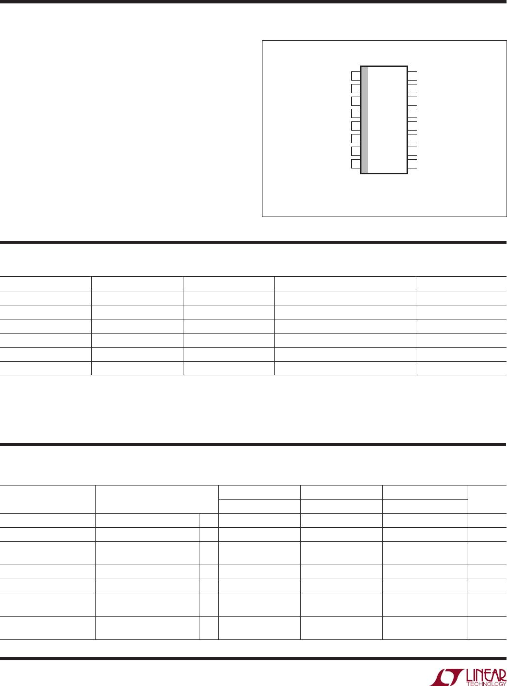
PIN CONFIGURATIONABSOLUTE MAXIMUM RATINGS
(Note 1, 2)
TOP VIEW
GN PACKAGE
16-LEAD NARROW PLASTIC SSOP
1
2
3
4
5
6
7
8
16
15
14
13
12
11
10
9
CH0
CH1
CH2
CH3
CH4
CH5
CH6
CH7/COM
V
DD
GND
SDI
SDO
SCK
CS/CONV
V
REF
REFCOMP
T
JMAX
= 110°C, θ
JA
= 95°C/W
CONVERTER CHARACTERISTICS
ORDER INFORMATION
LEAD FREE FINISH TAPE AND REEL PART MARKING* PACKAGE DESCRIPTION TEMPERATURE RANGE
LTC1863CGN#PBF LTC1863CGN#TRPBF 1863 16-Lead Narrow Plastic SSOP 0°C to 70°C
LTC1863IGN#PBF LTC1863IGN#TRPBF 1863 16-Lead Narrow Plastic SSOP –40°C to 85°C
LTC1867CGN#PBF LTC1867CGN#TRPBF 1867 16-Lead Narrow Plastic SSOP 0°C to 70°C
LTC1867IGN#PBF LTC1867IGN#TRPBF 1867 16-Lead Narrow Plastic SSOP –40°C to 85°C
LTC1867ACGN#PBF LTC1867ACGN#TRPBF 1867 16-Lead
Narrow Plastic SSOP 0°C to 70°C
LTC1867AIGN #PBF LTC1867AIGN#TRPBF 1867 16-Lead Narrow Plastic SSOP –40°C to 85°C
Consult LTC Marketing for parts specified with wider operating temperature ranges. *The temperature grade is identified by a label on the shipping container.
Consult LT C Marketing for information on non-standard lead based finish parts.
For more information on lead free part marking, go to: http://www.linear.
com/leadfree/
For more information on tape and reel specifications, go to: http://www.linear.com/tapeandreel/
Supply Voltage (V
DD
) ................................... 0.3V to 6V
Analog Input Voltage
CH0-CH7/COM (Note 3) ........... 0.3V to (V
DD
+ 0.3V)
V
REF
, REFCOMP (Note 4) ......... 0.3V to (V
DD
+ 0.3V)
Digital Input Voltage (SDI, SCK, CS/CONV)
(Note 4) ................................................. 0.3V to 10V
Digital Output Voltage (SDO)
....... 0.3V to (V
DD
+ 0.3V)
Power Dissipation .............................................. 500mW
Operating Temperature Range
LTC1863C/LTC1867C/LTC1867AC ............ C to 70°C
LTC1863I/LTC1867I/LTC1867AI ...........40°C to 8C
Storage Temperature Range .................. 6C to 150°C
Lead Temperature (Soldering, 10 sec) ................... 300°C
The l denotes the specifications which apply over the full operating
temperature range, otherwise specifications are at T
A
= 25°C. With external reference (Notes 5, 6)
PARAMETER CONDITIONS
LTC1863 LTC1867 LTC1867A
UNITSMIN TYP MAX MIN TYP MAX MIN TYP MAX
Resolution
l
12 16 16 Bits
No Missing Codes
l
12 15 16 Bits
Integral Linearity Error Unipolar (Note 7)
Bipolar
l
l
±1
±1
±4
±4
±2
±2.5
LSB
LSB
Differential Linearity Error
l
±1 –2 3 –1 1.75 LSB
Transition Noise 0.1 0.74 0.74 LSB
RMS
Offset Error Unipolar (Note 8)
Bipolar
l
l
±3
±4
±32
±64
±32
±64
LSB
LSB
Offset Error Match Unipolar
Bipolar
±1
±1
±2
±2
±2
±2
LSB
LSB
LTC1863/LTC1867
3
18637fc
For more information www.linear.com/LTC1863
SYMBOL PARAMETER CONDITIONS
LTC1863 LTC1867/LTC1867A
UNITSMIN TYP MAX MIN TYP MAX
SNR Signal-to-Noise Ratio 1kHz Input Signal
73.6 89 dB
S/(N+D) Signal-to-(Noise + Distortion) Ratio 1kHz Input Signal 73.5 88 dB
THD Total Harmonic Distortion 1kHz Input Signal, Up to 5th Harmonic –94.5 –95 dB
Peak Harmonic or Spurious Noise 1kHz Input Signal –94.5 –95 dB
Channel-to-Channel Isolation 100kHz Input Signal –100 –117 dB
Full Power Bandwidth –3dB Point 1.25 1.25 MHz
DYNAMIC ACCURACY
SYMBOL PARAMETER CONDITIONS
LTC1863/LTC1867/LTC1867A
UNITSMIN TYP MAX
Analog Input Range Unipolar Mode (Note
9)
Bipolar Mode
l
l
0-4.096
±2.048
V
V
C
IN
Analog Input Capacitance for CH0 to
CH7/COM
Between Conversions (Sample Mode)
During Conversions (Hold Mode)
32
4
pF
pF
t
ACQ
Sample-and-Hold Acquisition Time
l
1.5 1.1 µs
Input Leakage Current On Channels, CHX = 0V or V
DD
l
±1 µA
ANALOG INPUT
The l denotes the specifications which apply over the full operating temperature range, otherwise
specifications are at T
A
= 25°C. (Note 5)
PARAMETER CONDITIONS
LTC1863/LTC1867/LTC1867A
UNITSMIN TYP MAX
V
REF
Output Voltage I
OUT
= 0 2.48 2.5 2.52 V
V
REF
Output Tempco I
OUT
= 0 ±15 ppm/°C
V
REF
Line Regulation 4.75V ≤ V
DD
≤ 5.25V 0.43 mV/V
V
REF
Output Resistance I
OUT
≤0.1mA 6
REFCOMP Output Voltage I
OUT
= 0 4.096 V
INTERNAL REFERENCE CHARACTERISTICS
(Note 5)
CONVERTER CHARACTERISTICS
The l denotes the specifications which apply over the full operating
temperature range, otherwise specifications are at T
A
= 25°C. With external reference (Notes 5, 6)
PARAMETER CONDITIONS
LTC1863 LTC1867 LTC1867A
UNITSMIN TYP MAX MIN TYP MAX MIN TYP MAX
Offset Error Drift ±0.5 ±0.5 ±0.5 ppm/°C
Gain Error Unipolar
Bipolar
±6
±6
±96
±96
±64
±64
LSB
LSB
Gain Error Match ±1 ±4 ±2 LSB
Gain Error Tempco Internal Reference
External Reference
±15
±2.7
±15
±2.7
±15
±2.7
ppm/°C
ppm/°C
Power Supply Sensitivity V
DD
= 4.75V – 5.25V ±1 ±5 ±5 LSB
(Note 5)

LTC1863CGN#PBF

Mfr. #:
Manufacturer:
Analog Devices Inc.
Description:
Analog to Digital Converters - ADC 12-bit, 8-ch. Serial, Micropower ADC
Lifecycle:
New from this manufacturer.
Delivery:
DHL FedEx Ups TNT EMS
Payment:
T/T Paypal Visa MoneyGram Western Union