LTC1863/LTC1867
7
18637fc
For more information www.linear.com/LTC1863
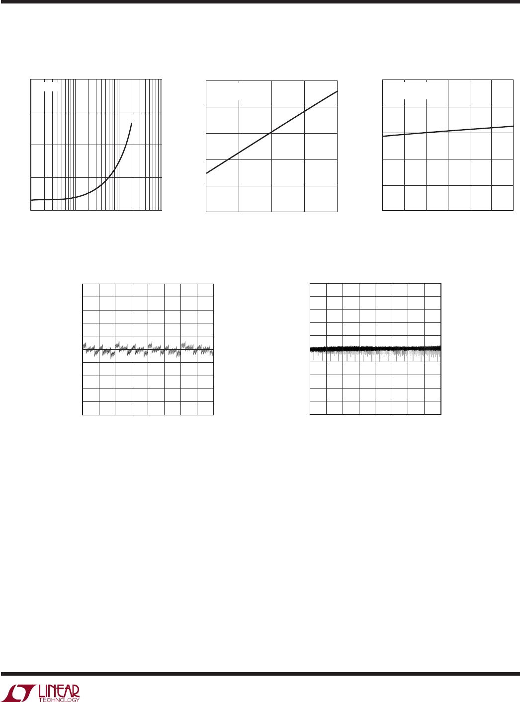
TYPICAL PERFORMANCE CHARACTERISTICS
(LTC1863/LTC1867)
Supply Current vs f
SAMPLE
Supply Current vs Supply Voltage Supply Current vs Temperature
Differential Nonlinearity vs
Output Code (LTC1863)
Integral Nonlinearity vs Output
Code (LTC1863)
f
SAMPLE
(ksps)
1
SUPPLY CURRENT (mA)
2.0
1.5
1.0
0.5
0
10 100 1000
18637 G10
V
DD
= 5V
SUPPLY VOLTAGE (V)
4.5
SUPPLY CURRENT (mA)
5.5
18637 G11
4.75
5.0
5.25
1.5
1.4
1.3
1.2
1.1
1.0
V
DD
= 5V
f
SAMPLE
= 200ksps
TEMPERATURE (°C)
–50
SUPPLY CURRENT (mA)
1.5
1.4
1.3
1.2
1.1
1.0
–25
0 25 50
18637 G12
75 100
V
DD
= 5V
f
SAMPLE
= 200ksps
OUTPUT CODE
0
INL (LBS)
1.0
0.8
0.6
0.4
0.2
0
–0.2
–0.4
–0.6
–0.8
–1.0
1024
2048
2560
18637 G13
512 1536
3072
3584
4096
OUTPUT CODE
0
DNL (LBS)
1.0
0.8
0.6
0.4
0.2
0
–0.2
–0.4
–0.6
–0.8
–1.0
1024
2048
2560
18637 G14
512 1536
3072
3584
4096
LTC1863/LTC1867
8
18637fc
For more information www.linear.com/LTC1863
PIN FUNCTIONS
TYPICAL CONNECTION DIAGRAM
TEST CIRCUITS
3k
(A) Hi-Z TO V
OH
AND V
OL
TO V
OH
C
L
3k
5V
DNDN
(B) Hi-Z TO V
OL
AND V
OH
TO V
OL
C
L
18637 TC01
3k
(A) V
OH
TO Hi-Z
C
L
3k
5V
DNDN
(B) V
OL
TO Hi-Z
C
L
18637 TC02
Load Circuits for Access Timing Load Circuits for Output Float Delay
CH0
CH1
CH2
CH3
CH4
CH5
CH6
CH7/COM
V
DD
GND
SDI
SDO
SCK
CS/CONV
V
REF
REFCOMP
LTC1863/
LTC1867
+
+
DIGITAL
I/O
5V
4.096V
10µF
2.2µF
2.5V
±2.048V
DIFFERENTIAL
INPUTS
4.096V
SINGLE-ENDED
INPUT
18637 TCD
CHO-CH7/COM (Pins 1-8): Analog Input Pins. Analog
inputs must be free of noise with respect to GND. CH7/
COM can be either a separate channel or the common
minus input for the other channels.
REFCOMP (Pin 9): Reference Buffer Output Pin. Bypass
to GND with 10µF tantalum capacitor in parallel with
0.1µF ceramic capacitor (4.096V Nominal). To overdrive
REFCOMP, tie V
REF
to GND.
V
REF
(Pin 10): 2.5V Reference Output. This pin can also
be used as an external reference buffer input for improved
accuracy and drift. Bypass to GND with 2.2µF tantalum
capacitor in parallel with 0.1µF ceramic capacitor.
CS/CONV (Pin 11): This input provides the dual function
of initiating conversions on the ADC and also frames the
serial data transfer.
SCK (Pin 12): Shift Clock. This clock synchronizes the
serial data transfer
.
SDO (Pin 13): Digital Data Output. The A/D conversion
result is shifted out of this output. Straight binary format
for unipolar mode and two’s complement format for
bipolar mode.
SDI (Pin 14): Digital Data Input Pin. The A/D configuration
word is shifted into this input.
GND (Pin 15): Analog and Digital GND.
V
DD
(Pin 16): Analog and Digital Power Supply. Bypass to
GND with 10µF
tantalum capacitor in parallel with 0.1µF
ceramic capacitor.
LTC1863/LTC1867
9
18637fc
For more information www.linear.com/LTC1863
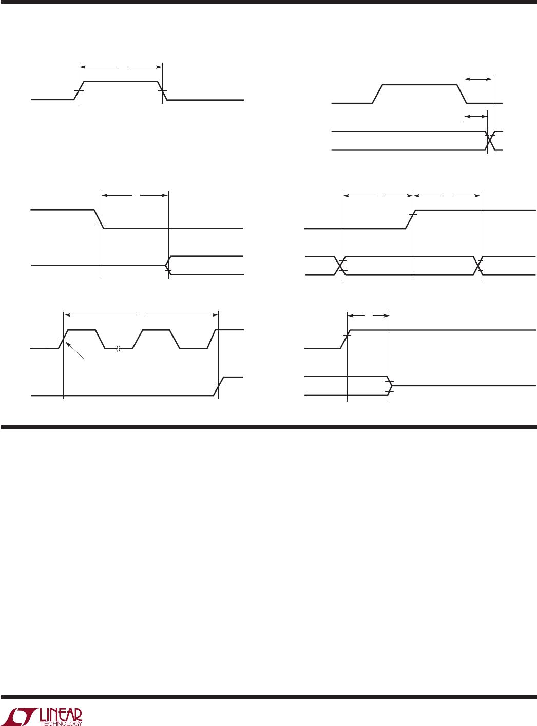
TIMING DIAGRAMS
t
5
(SDI Setup Time Before SCK),
t
6
(SDI Hold Time After SCK)
50%
50%
t
3
0.4V
t
7
(SLEEP Mode Wake-Up Time)
t
7
SCK
CS/CONV
t
8
(BUS Relinquish Time)
t
8
CS/CONV
SDO
2.4V
t
4
(SDO Valid After CONV)
t
4
CS/CONV
SDO
2.4V
0.4V
0.4V
t
6
2.4V
0.4V
t
5
SCK
SDI
2.4V
2.4V
0.4V
2.4V
0.4V
SDO
1867 TD
SLEEP BIT (SLP = 0)
READ-IN
10%
90%
Hi-Z
Hi-Z
t
1
(For Short Pulse Mode)
t
2
(SDO Valid Before SCK),
t
3
(SDO Valid Hold Time After SCK)
t
1
CS/CONV
t
2
SCK
50%
50%
Overview
The LTC1863/LTC1867 are complete, low power multi-
plexed ADCs. They consist of a 12-/16-bit, 200ksps capaci-
tive successive approximation A/D converter, a precision
internal reference, a configurable 8-channel analog input
multiplexer (MUX) and a serial port for data transfer.
Conversions are started by a rising edge on the CS/CONV
input. Once a conversion cycle has begun, it cannot be
restarted. Between conversions, the
ADCs receive an input
word for channel selection and output the conversion
result, and the analog input is acquired in preparation for
the next conversion. In the acquire phase, a minimum time
of 1.5µs will provide enough time for the sample-and-hold
capacitors to acquire the analog signal.
During the conversion, the internal differential 16-bit
capacitive DAC output is sequenced by the SAR from
the most
significant bit (MSB) to the least significant bit
(LSB). The input is successively compared with the binary
weighted charges supplied by the differential capacitive
DAC. Bit decisions are made by a low-power, differential
comparator. At the end of a conversion, the DAC output
balances the analog input. The SAR contents (a 12-/16-bit
data word) that represent the analog input are loaded into
the 12-/16-bit output
latches.
APPLICATIONS INFORMATION
LTC1863CGN#PBF

Mfr. #:
Manufacturer:
Analog Devices Inc.
Description:
Analog to Digital Converters - ADC 12-bit, 8-ch. Serial, Micropower ADC
Lifecycle:
New from this manufacturer.
Delivery:
DHL FedEx Ups TNT EMS
Payment:
T/T Paypal Visa MoneyGram Western Union