LTC1863/LTC1867
10
18637fc
For more information www.linear.com/LTC1863
APPLICATIONS INFORMATION
Examples of Multiplexer Options
CH0
CH1
CH2
CH3
CH4
CH5
CH6
CH7/COM
GND (
)
8 Single-Ended
+
+
+
+
+
+
+
4 Differential
+
(
)
+
CH0
CH1
CH2
CH3
CH4
CH5
CH6
CH7/COM (
)
7 Single-Ended
to CH7/COM
+
+
+
+
+
+
+
+
(
)
+
(
)
+
(
)
(
+
)
(
+
)
(
+
)
(
+
)
GND (
)
Combinations of Differential
and Single-Ended
+
+
+
+
+
+
{
{
{
{
{
{
18637 AI01
CH0
CH1
CH2
CH3
CH4
CH5
CH6
CH7/COM
CH0
CH1
CH2
CH3
CH4
CH5
CH6
CH7/COM
Analog Input Multiplexer
The analog input multiplexer is controlled by a 7-bit input
data word. The input data word is defined as follows:
SD OS S1 S0 COM UNI SLP
SD = SINGLE/DIFFERENTIAL BIT
OS = ODD/SIGN BIT
S1 = ADDRESS SELECT BIT 1
S0 = ADDRESS SELECT BIT 0
COM = CH7/COM CONFIGURATION BIT
UNI = UNIPOLAR/BIPOLAR BIT
SLP = SLEEP MODE BIT
Tables 1 and 2 show the configurations when COM = 0,
and COM = 1.
Table 1. Channel Configuration (When COM = 0, CH7/COM Pin
Is Used as CH7)
Channel Configuration
SD OS S1 S0 COM “+” “–”
0 0 0 0 0 CH0 CH1
0 0 0 1 0 CH2 CH3
0 0 1 0 0 CH4 CH5
0 0 1 1 0 CH6 CH7
0 1 0 0 0 CH1 CH0
0 1 0 1 0 CH3 CH2
0 1 1 0 0 CH5 CH4
0 1 1 1 0 CH7 CH6
1 0 0 0 0 CH0 GND
1 0 0 1 0 CH2 GND
1 0 1 0 0 CH4 GND
1
0 1 1 0 CH6 GND
1 1 0 0 0 CH1 GND
1 1 0 1 0 CH3 GND
1 1 1 0 0 CH5 GND
1 1 1 1 0 CH7 GND
Table 2. Channel Configuration (When COM = 1, CH7/COM Pin
Is Used as COMMON)
Channel Configuration
SD OS S1 S0 COM “+” “–”
1 0 0 0 1 CH0 CH7/COM
1 0 0 1 1 CH2 CH7/COM
1 0 1 0 1 CH4 CH7/COM
1 0 1 1 1 CH6 CH7/COM
1 1 0 0 1 CH1 CH7/COM
1 1 0 1 1 CH3 CH7/COM
1 1 1 0 1 CH5 CH7/COM
Changing the MUX Assignment “On the Fly”
CH7/COM
(UNUSED)
CH7/COM (
)
1st Conversion 2nd Conversion
+
+
+
+
+
{
{
{
{
CH2
CH3
CH4
CH5
CH2
CH3
CH4
CH5
18637 AI02
LTC1863/LTC1867
11
18637fc
For more information www.linear.com/LTC1863
Driving the Analog Inputs
The analog inputs of the LTC1863/LTC1867 are easy to
drive. Each of the analog inputs can be used as a single-
ended input relative to the GND pin (CH0-GND, CH1-GND,
etc) or in pairs (CH0 and CH1, CH2 and CH3, CH4 and CH5,
CH6 and CH7) for differential inputs. In addition, CH7 can
act as a COM pin for both
single-ended and differential
modes if the COM bit in the input word is high. Regard-
less of the MUX configuration, the “+” and “–” inputs are
sampled at the same instant. Any unwanted signal that is
common mode to both inputs will be reduced by the com-
mon mode rejection of the sample-and-hold circuit. The
inputs draw only one small current spike while charging
the sample
-and-hold capacitors during the acquire mode.
In conversion mode, the analog inputs draw only a small
leakage current. If the source impedance of the driving
circuit is low then the LTC1863/LTC1867 inputs can be
driven directly. More acquisition time should be allowed
for a higher impedance source.
The following list is a summary of the op amps that are
suitable for driving the LTC
1863/LTC1867. More detailed
information is available in the Linear Technology data books
or Linear Technology website.
LT1007 - Low noise precision amplifier. 2.7mA supply
current ± 5V to ±15V supplies. Gain bandwidth product
8MHz. DC applications.
LT1097 - Low cost, low power precision amplifier. 300µA
supply current. ±5V to ±15V supplies. Gain bandwidth
product 0.7MHz. DC applications.
LT1227 - 140MHz video current feedback amplifier. 10mA
supply current. ±5V to ±15V supplies. Low noise and low
distortion.
LT1360 - 37MHz voltage feedback amplifier. 3.8mA supply
current. ±5V to ±15V supplies. Good AC/DC specs.
LT1363 - 50MHz voltage feedback amplifier. 6.3mA supply
current. Good AC/DC specs.
LT1364/LT1365 - Dual and quad 50MHz voltage feedback
amplifiers. 6.3mA supply current per amplifier. Good
AC/DC specs.
LT1468 - 90MHz, 22V/µs 16-bit accurate amplifier
LT1469 - Dual LT1468
Input Filtering
The noise and the distortion of the input amplifier and
other circuitry must be considered since they will add to
the LTC1863/LTC1867 noise and distortion. Noisy input
circuitry should be filtered prior to the analog inputs to
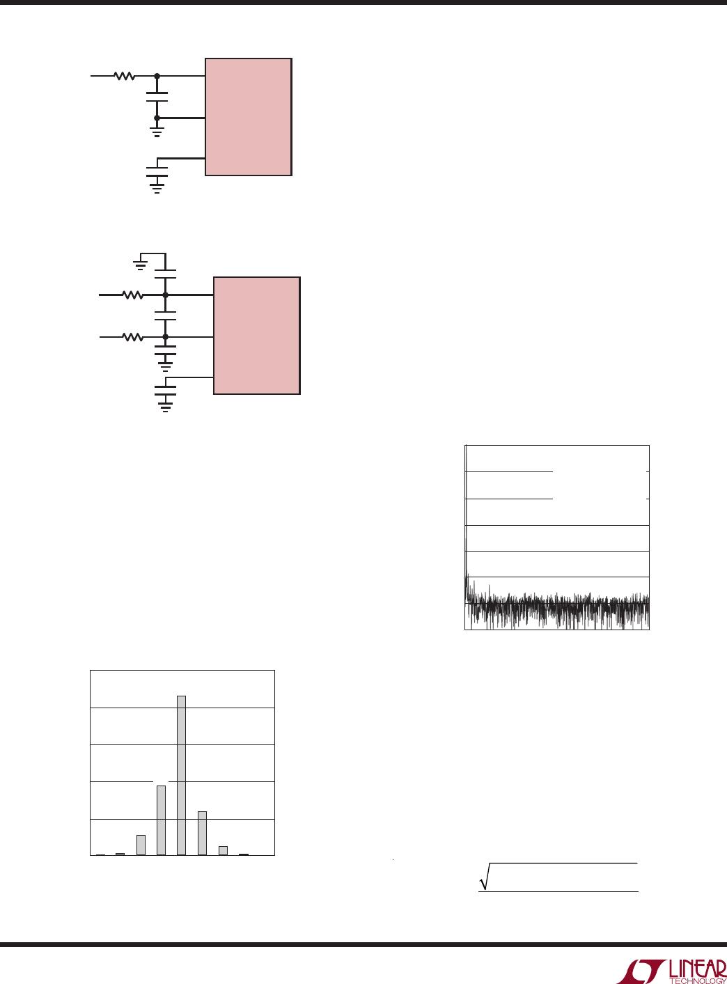
minimize noise. A simple 1-pole RC filter is sufficient for
many applications. For instance, Figure 1 shows a 50Ω
source resistor and a 2000pF capacitor
to ground on the
input will limit the input bandwidth to 1.6MHz. The source
impedance has to be kept low to avoid gain error and
degradation in the AC performance. The capacitor also
acts as a charge reservoir for the input sample-and-hold
and isolates the ADC input from sampling glitch sensitive
circuitry. High quality capacitors and resistors should be
used since these components can add
distortion. NPO
and silver mica type dielectric capacitors have excellent
linearity. Carbon surface mount resistors can also generate
distortion from self heating and from damage that may
occur during soldering. Metal film surface mount resistors
are much less susceptible to both problems.
APPLICATIONS INFORMATION
LTC1863/LTC1867
12
18637fc
For more information www.linear.com/LTC1863
APPLICATIONS INFORMATION
DC Performance
One way of measuring the transition noise associated
with a high resolution ADC is to use a technique where
a DC signal is applied to the input of the ADC and the
resulting output codes are collected over a large number
of conversions. For example, in Figure 2 the distribution
of output codes is shown for a DC input that had been
digitized 4096 times. The
distribution is Gaussian and the
RMS code transition noise is about 0.74LSB.
1867 F01a
CH0
GND
LTC1863/
LTC1867
REFCOMP
2000pF
10µF
50Ω
ANALOG
INPUT
1000pF
1867 F01b
CH0
CH1
LTC1863/
LTC1867
REFCOMP
1000pF
1000pF
10µF
50Ω
50Ω
DIFFERENTIAL
ANALOG
INPUTS
Figure 1a. Optional RC Input Filtering for Single-Ended Input
Figure 1b. Optional RC Input Filtering for Differential Inputs
Figure 2. LTC1867 Histogram for 4096 Conversions
Dynamic Performance
FFT (Fast Fourier Transform) test techniques are used to
test the ADC’s frequency response, distortion and noise
at the rated throughput. By applying a low distortion
sine wave and analyzing the digital output using an FFT
algorithm, the ADC’s spectral content
can be examined
for frequencies outside the fundamental.
Signal-to-Noise Ratio
The Signal-to-Noise and Distortion Ratio (SINAD) is the
ratio between the RMS amplitude of the fundamental input
frequency to the RMS amplitude of all other frequency
components at the A/D output. The output is band limited
to frequencies from above DC and below half the sampling
frequency. Figure 3 shows a typical SINAD
of 87.9dB
with a 200kHz sampling rate and a 1kHz input. When an
external 5V is applied to REFCOMP (tie V
REF
to GND), a
signal-to-noise ratio of 90dB can be achieved.
CODE
–4
COUNTS
4
18637 GO3
–2–3
0–1
321
2500
2000
1500
1000
500
0
1
26
276
2152
579
122
5
0
935
Figure 3. LTC1867 Nonaveraged 4096 Point FFT Plot
FREQUENCY (kHz)
0
0
–20
–40
–60
–80
–100
–120
–140
75
18637 G04
25 50 100
AMPLITUDE (dB)
SNR = 88.8dB
SINAD = 87.9dB
THD = 95dB
f
SAMPLE
= 200ksps
INTERNAL REFERENCE
Total Harmonic Distortion
Total Harmonic Distortion (THD) is the ratio of the RMS
sum of all harmonics of the input signal to the fundamental
itself. The out-of-band harmonics alias into the frequency
band between DC and half the sampling frequency. THD
is expressed as:
THD = 20log
V
2
2
+ V
3
2
+ V
4
2
...+ V
N
2
V
1

LTC1863CGN#PBF

Mfr. #:
Manufacturer:
Analog Devices Inc.
Description:
Analog to Digital Converters - ADC 12-bit, 8-ch. Serial, Micropower ADC
Lifecycle:
New from this manufacturer.
Delivery:
DHL FedEx Ups TNT EMS
Payment:
T/T Paypal Visa MoneyGram Western Union