LTC1863/LTC1867
14
18637fc
For more information www.linear.com/LTC1863
APPLICATIONS INFORMATION
If the CS/CONV returns low during a bit decision, it can
create a small error. For best performance ensure that
the CS/CONV returns low either within 100ns after the
conversion starts (i.e. before the first bit decision) or
after the conversion ends. If CS/CONV is low when the
conversion ends, the MSB bit will appear on SDO at the
end of the
conversion and the ADC will remain powered
up (see Figure 7).
Sleep Mode
If the SLP = 1 is selected in the input word, the ADC
will enter SLEEP mode and draw only leakage current
(provided that all the digital inputs stay at GND or V
DD
).
After release from the SLEEP mode, the ADC need 60ms
to wake up (2.2µF/10µF bypass capacitors on V
REF
/
REFCOMP pins).
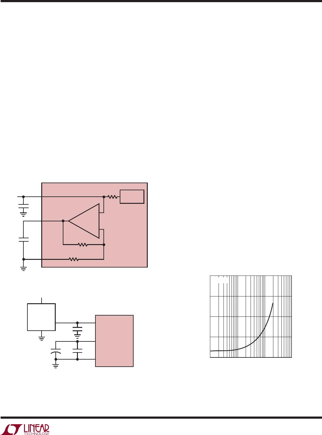
Board
Layout and Bypassing
To obtain the best performance, a printed circuit board
with a ground plane is required. Layout for the printed
circuit board should ensure digital and analog signal lines
are separated as much as possible. In particular, care
should be taken not to run any digital signal alongside
an analog signal.
All analog inputs should be screened by GND. V
REF
,
REFCOMP and V
DD
should be bypassed to this ground
plane as close to the pin as possible; the low impedance
of the common return for these bypass capacitors is es-
sential to the low noise operation of the ADC. The width
for these tracks should be as wide as possible.
Timing and Control
Conversion start is controlled by the CS/CONV digital in-
put. The rising edge transition of the CS/CONV
will start a
conversion. Once initiated, it cannot be restarted until the
conversion is complete. Figures 6 and 7 show the timing
diagrams for two types of CS/CONV pulses.
Example 1 (Figure 6) shows the LTC1863/LTC1867 operat-
ing in automatic nap mode with CS/CONV signal staying
HIGH after the conversion. Automatic nap mode provides
power reduction at reduced sample rate. The ADCs can also
operate with the
CS/CONV signal returning LOW before
the conversion ends. In this mode (Example 2, Figure 7),
the ADCs remain powered up.
For best performance, it is recommended to keep SCK, SDI,
and SDO at a constant logic high or low during acquisition
and conversion, even though these signals may be ignored
by the serial interface (DON’T CARE). Communication
with other devices on the bus should not coincide with
the conversion period (t
CONV
).
Figures 8 and 9 are the transfer characteristics for the
bipolar and unipolar mode.
S0SD 0S S1
COM
UNI SLP
D11 D10 D9 D8 D7 D6 D5 D4 D3 D2 D1 D0
1/f
SCK
t
ACQ
CS/CONV
SCK
SDI
SDO
(LTC1863)
Hi-Z
D12D15 D14 D13 D11 D10 D9 D8 D7 D6 D5 D4 D3 D2 D1 D0
Hi-Z
1 2 3 4 5 6 7 8 9 10 11 12 13 14 15 16
1867 F06
DON'T CARE
NOT NEEDED FOR LTC1863
t
CONV
NAP MODE
SDO
(LTC1867)
MSB
MSB
DON'T CARE
DON'T CARE
DON'T CARE
Figure 6. Example 1, CS/CONV Starts a Conversion and Remains HIGH Until Next Data Transfer. With CS/CONV Remaining HIGH After
the Conversion, Automatic Nap Modes Provides Power Reduction at Reduced Sample Rate.