AD7892
REV. C
–9–
CIRCUIT DESCRIPTION
The AD7892 is a fast, 12-bit single supply A/D converter. It
provides the user with signal scaling, track/hold, reference, A/D
converter and versatile interface logic functions on a single chip.
The signal scaling on the AD7892-1 allows the part to handle
either ± 5 V or ± 10 V input signals while operating from a single
+5 V supply. The AD7892-2 handles a 0 V to +2.5 V analog
input range, while signal scaling on the AD7892-3 allows it to
handle ± 2.5 V input signals when operating from a single supply.
The part requires a +2.5 V reference which can be provided from
the part’s own internal reference or from an external reference
source.
Conversion is initiated on the AD7892 by pulsing the CONVST
input. On the rising edge of CONVST, the track/hold goes
from track mode to hold mode and the conversion sequence is
started. At the end of conversion (falling edge of EOC), the
track/hold returns to tracking mode and the acquisition time
begins. Conversion time for the part is 1.47 µs (AD7892-3) and
the track/hold acquisition time is 200 ns (AD7892-3). This allows
the AD7892-3 to operate at throughput rates up to 600 kSPS.
The AD7892-1 and AD7892-2 are specified with a 1.6 µs con-
version and 400 ns acquisition time allowing a throughput rate
of 500 kSPS.
Track/Hold Section
The track/hold amplifier on the AD7892 allows the ADC to
accurately convert an input sine wave of full-scale amplitude to
12-bit accuracy. The input bandwidth of the track/hold is greater
than the Nyquist rate of the ADC even when the ADC is oper-
ated at its maximum throughput rate of 600 kHz (i.e., the track/
hold can handle input frequencies in excess of 300 kHz).
The track/hold amplifier acquires an input signal to 12-bit accu-
racy in less than 200 ns. The operation of the track/hold is
essentially transparent to the user. The track/hold amplifier
goes from its tracking mode to its hold mode on the rising edge
of CONVST. The aperture time for the track/hold (i.e., the
delay time between the external CONVST signal and the track/
hold actually going into hold) is typically 15 ns. At the end of
conversion, the part returns to its tracking mode. The acquisi-
tion time of the track/hold amplifier begins at this point.
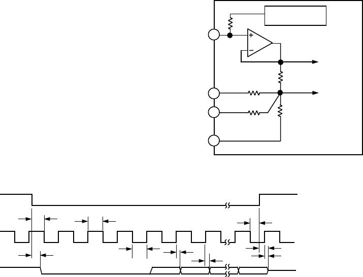
Reference Section
The AD7892 contains a single reference pin, labelled REF OUT/
REF IN, which either provides access to the part’s own +2.5 V
reference or to which an external +2.5 V reference can be con-
nected to provide the reference source for the part. The part is
specified with a +2.5 V reference voltage. Errors in the refer-
ence source will result in gain errors in the AD7892’s transfer
function and will add to the specified full-scale errors on the
part. On the AD7892-1 and AD7892-3, it will also result in an
offset error injected in the attenuator stage.
The AD7892 contains an on-chip +2.5 V reference. To use this
reference as the reference source for the AD7892, simply con-
nect a 0.1 µF disc ceramic capacitor from the REF OUT/
REF IN pin to AGND. The voltage that appears at this pin is
internally buffered before being applied to the ADC. If this
reference is required for use external to the AD7892, it should
be buffered as the part has a FET switch in series with the refer-
ence output resulting in a source impedance for this output of
5.5 k nominal. The tolerance on the internal reference is
± 10 mV at 25°C with a typical temperature coefficient of
25 ppm/°C and a maximum error over temperature of ± 25 mV.
If the application requires a reference with a tighter tolerance or
the AD7892 needs to be used with a system reference, then the
user has the option of connecting an external reference to this
REF OUT/REF IN pin. The external reference will effectively
overdrive the internal reference and thus provide the reference
source for the ADC. The reference input is buffered before
being applied to the ADC with the maximum input current is
± 100 µA. Suitable reference sources for the AD7892 include the
AD680, AD780 and REF43 precision +2.5 V references.
INTERFACING
The part provides two interface options, a 12-bit parallel inter-
face and a three-wire serial interface. The required interface
mode is selected via the MODE pin. The two interface modes
are discussed in the following sections.
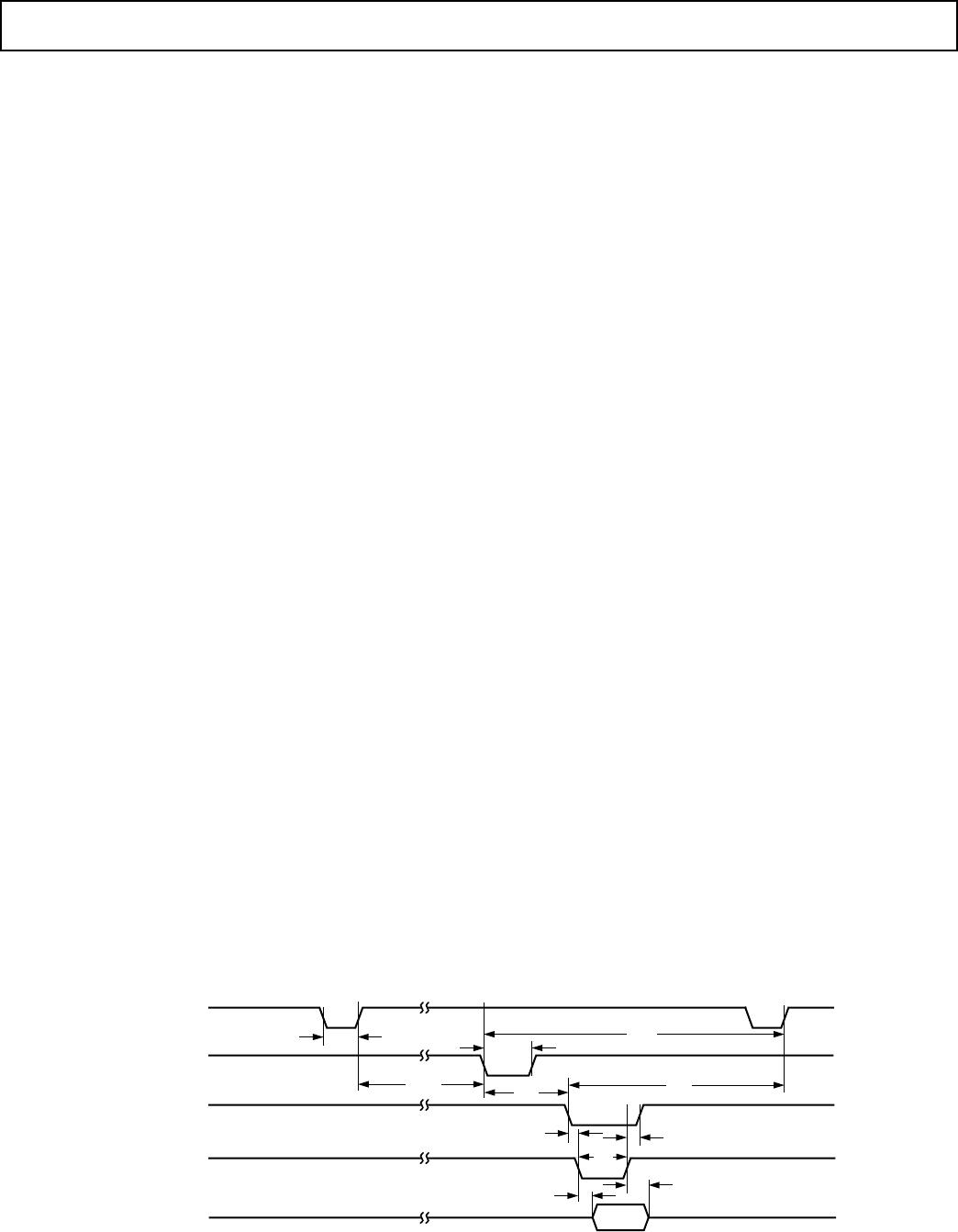
Parallel Interface Mode
The parallel interface mode is selected by tying the MODE
input to a logic high. Figure 2 shows a timing diagram illustrat-
ing the operational sequence of the AD7892. The on-chip
track/hold goes into hold mode, and conversion is initiated on
the rising edge of the CONVST signal. When conversion is
complete, the end of conversion line (EOC) pulses low to indi-
cate that new data is available in the AD7892’s output register.
This EOC line can be used to drive an edge-triggered interrupt
of a microprocessor. The falling edge of the RD signal should
occur 200 ns prior to the next rising edge of CONVST. CS and
RD going low accesses the 12-bit conversion result. In systems
where the part is interfaced to a gate array or ASIC, this EOC
VALID
DATA
t
CONV
t
8
t
5
t
4
t
7
t
6
t
2
t
1
THREE-STATE
CONVST (I)
EOC (O)
CS (I)
RD (I)
DB0–DB11 (O)
NOTE:
I = INPUT; O = OUTPUT
t
ACQ
t
3
t
9
THREE-STATE
Figure 2. Parallel Mode Timing Diagram
AD7892
–10–
REV. C
pulse can be applied to the CS and RD inputs to latch data out
of the AD7892 and into the gate array or ASIC. This eliminates
the logic required in the gate array or ASIC to recognize the end
of conversion and generate the read signal for the AD7892. To
obtain optimum performance from the AD7892, it is not recom-
mended to tie CS and RD permanently low as this keeps the
three-state active during conversion.
Serial Interface Mode
The AD7892 is configured for serial mode interfacing by tying
the MODE input low. It provides for a three-wire, serial link
between the AD7892 and industry-standard microprocessors,
microcontrollers and digital signal processors. SCLK and RFS
of the AD7892 are inputs, and the AD7892’s serial interface is
designed for direct interface to systems that provide a serial
clock input that is synchronized to the serial data output includ-
ing microcontrollers such as the 80C51, 87C51, 68HC11 and
68HC05 and most digital signal processors.
Figure 3 shows the timing diagram for reading from the AD7892
in the serial interface mode. RFS goes low to access data from
the AD7892. The serial clock input does not have to be con-
tinuous. The serial data can be accessed in a number of bytes.
However, RFS must remain low for the duration of the data
transfer operation. Sixteen bits of data are transmitted with four
leading zeros followed by the 12-bit conversion result starting
with the MSB. Serial data is clocked out of the device on the
rising edge of SCLK. Old data is guaranteed to be valid for 5 ns
after this edge. This is useful for high speed serial clocks where
the access time of the part would not allow sufficient set-up time
for the data to be accepted on the falling edge of the clock. In
this case, care must be taken that RFS does not go just prior to
a rising edge of SCLK. For slower serial clocks data is valid on
the falling edge of SCLK. At the end of the read operation, the
SDATA line is three-stated by a rising edge on either the SCLK
or RFS inputs, whichever occurs first. Serial data cannot be
read during conversion to avoid feedthrough problems from the
serial clock to the conversion process. For optimum perfor-
mance of the AD7892-3, a serial read should also be avoided
within 200 ns of the rising edge of CONVST to avoid feedthrough
into the track/hold during its acquisition time. The serial read
should, therefore, occur between the end of conversion (EOC
falling edge) and 200 ns prior to the next rising edge of
CONVST. For the AD7892-1 and AD7892-2, a serial read
should also be avoided within 400 ns of the rising edge of
CONVST. This limits the maximum achievable throughput
rate in serial mode (assuming 20 MHz serial clock) to 400 kSPS
for the AD7892-3 and 357 kSPS for the AD7892-1 and
AD7892-2.
Analog Input Section
The AD7892 is offered as three part types allowing for four
different analog input voltage ranges. The AD7892-1 handles
either ± 5 V or ± 10 V input voltage ranges. The AD7892-2
handles a 0 V to +2.5 V input voltage range while the AD7892-3
handles an input range of ± 2.5 V.
AD7892-1
Figure 4 shows the analog input section for the AD7892-1. The
analog input range is pin-strappable (using V
IN2
) for either ± 5V
or ± 10 V on the V
IN1
input. With V
IN2
connected to AGND, the
input range on V
IN1
is ± 10 V, and the input resistance on V
IN1
is
15 k nominal. With V
IN2
connected to V
IN1
, the input range on
V
IN1
is ± 5 V, and the input resistance on V
IN1
is 8 k nominal.
As a result, the V
IN1
and V
IN2
inputs should be driven from a
low impedance source. The resistor attenuator stage is followed
by the high input impedance stage of the track/hold amplifier.
This resistor attenuator stage allows the input voltage to go to
± 17 V without damaging the AD7892-1.
+2.5
REFERENCE
REF OUT/
REF IN
V
IN1
V
IN2
AGND
TO HIGH
IMPEDANCE
SHA INPUT
TO ADC
REFERENCE
CIRCUITRY
2k
3.25k
13k
6.5k
13k
Figure 4. AD7892-1 Analog Input Structure
t
13
t
10
THREE-
STATE
RFS (I)
SCLK (I)
SDATA (O)
NOTE:
I = INPUT; O = OUTPUT
FOUR LEADING ZEROS
t
12
t
11
t
16
t
17
t
17A
t
14
DB11 DB10 DB0
t
15
Figure 3. Serial Mode Timing Diagram
AD7892
REV. C
–11–
The designed code transitions occur midway between successive
integer LSB values (i.e., 1/2 LSB, 3/2 LSBs, 5/2 LSBs). Output
coding is two’s complement binary with 1 LSB = FSR/4096 =
20 V/4096 = 4.88 mV for the ±10 V range and 1 LSB = FSR/
4096 = 10 V/4096 = 2.44 mV for the ± 5 V range. The ideal
input/output transfer function for the AD7892-1 is shown in
Table I.
AD7892-2
The analog input section for the AD7892-2 contains no biasing
resistors. The analog input looks directly into the track/hold
input stage. The analog input range on the V
IN1
input is 0 V to
+2.5 V. The V
IN2
input can be left unconnected but if it is
connected to a potential then that potential must be AGND.
The V
IN1
input connects directly to the input sampling capacitor
of the AD7892-2’s track/hold. The value of this input sampling
capacitor is nominally 10 pF.
Once again, the designed code transitions occur midway be-
tween successive integer LSB values (i.e., 1/2 LSB, 3/2 LSBs,
5/2 LSBs). Output coding is straight (natural) binary with
1 LSB = FSR/4096 = 2.5 V/4096 = 0.61 mV. The ideal input/
output transfer function for the AD7892-2 is shown in Table II.
Table I. Ideal Input/Output Code Table for the AD7892-1
Digital Output
Analog Input Code Transition
+FSR/2 – 3/2 LSB
1, 2
(9.99268 or 4.99634)
3
011 . . . 110 to 011 . . . 111
+FSR/2 – 5/2 LSBs (9.98779 or 4.99390) 011 . . . 101 to 011 . . . 110
+FSR/2 – 7/2 LSBs (9.98291 or 4.99146) 011 . . . 100 to 011 . . . 101
AGND + 3/2 LSB (0.00732 or 0.00366) 000 . . . 001 to 000 . . . 010
AGND + 1/2 LSB (0.00244 or 0.00122) 000 . . . 000 to 000 . . . 001
AGND – 1/2 LSB (–0.00244 or –0.00122) 111 . . . 111 to 000 . . . 000
AGND – 3/2 LSB (–0.00732 or –0.00366) 111 . . . 110 to 111 . . . 111
–FSR/2 + 5/2 LSB (–9.98779 or –4.99390) 100 . . . 010 to 100 . . . 011
–FSR/2 + 3/2 LSB (–9.99268 or –4.99634) 100 . . . 001 to 100 . . . 010
–FSR/2 + 1/2 LSB (–9.99756 or –4.99878) 100 . . . 000 to 100 . . . 001
NOTES
1
FSR is full-scale range and REF IN = +2.5 V, is 20 V for the ± 10 V range and 10 V
for the ± 5 V range.
2
1 LSB = FSR/4096 = 4.88 mV (± 10 V range) and 2.44 mV (± 5 V range) with REF
IN = +2.5 V.
3
± 10 V range or ± 5 V range.
Table II. Ideal Input/Output Code Table for the AD7892-2
Digital Output
Analog Input Code Transition
+FSR – 3/2 LSB
1, 2
(2.499084 V) 111 . . . 110 to 111 . . . 111
+FSR – 5/2 LSBs (2.498474 V) 111 . . . 110 to 111 . . . 110
+FSR – 7/2 LSBs (2.497864 V) 111 . . . 100 to 111 . . . 101
AGND + 5/2 LSB (0.001526 V) 000 . . . 010 to 010 . . . 011
AGND + 3/2 LSB (0.00916 V) 000 . . . 001 to 001 . . . 010
AGND + 1/2 LSB (0.000305 V) 000 . . . 000 to 000 . . . 001
NOTES
1
FSR is full-scale range and is 2.5 V with REF IN = +2.5 V.
2
1 LSB = FSR/4096 = 0.61 mV with REF IN = +2.5 V.
AD7892-3
Figure 5 shows the analog input section for the AD7892-3. The
analog input range is ±2.5 V on the V
IN1
input. The V
IN2
input
can be left unconnected but if it is connected to a potential then
that potential must be AGND. The input resistance on the V
IN1
is 1.8 k nominal. As a result, the V
IN1
input should be driven
from a low impedance source. The resistor attenuator stage is
followed by the high input impedance stage of the track/hold
amplifier. This resistor attenuator stage allows the input voltage
to go to ± 7 V without damaging the AD7892-3.
The designed code transitions occur midway between succes-
sive integer LSB values (i.e., 1/2 LSB, 3/2 LSBs, 5/2 LSBs).
Output coding is two’s complement binary with 1 LSB = FSR/
4096 = 5 V/4096 = 1.22 mV with REF IN = +2.5 V. The ideal
input/output transfer function for the AD7892-3 is shown in
Table III.
+2.5
REFERENCE
REF OUT/
REF IN
V
IN1
V
IN2
*
AGND
TO HIGH
IMPEDANCE
SHA INPUT
TO ADC
REFERENCE
CIRCUITRY
2k
3.25k
3.25k
* UNCONNECTED INTERNALLY ON THE AD7892-3
Figure 5. AD7892-3 Analog Input Structure
Table III. Ideal Input/Output Code Table for the AD7892-3
Digital Output
Analog Input Code Transition
+FSR/2 – 3/2 LSB
1, 2
(2.49817) 011 . . . 110 to 011 . . . 111
+FSR/2 – 5/2 LSBs (2.49695) 011 . . . 110 to 011 . . . 110
+FSR/2 – 7/2 LSBs (2.49573) 011 . . . 110 to 011 . . . 101
AGND + 3/2 LSB (0.00183) 000 . . . 001 to 000 . . . 010
AGND + 1/2 LSB (0.00061) 000 . . . 000 to 000 . . . 001
AGND – 1/2 LSB (–0.00061) 111 . . . 111 to 000 . . . 000
AGND – 3/2 LSB (–0.00183) 111 . . . 110 to 111 . . . 111
–FSR/2 + 5/2 LSB (–2.49695) 100 . . . 010 to 100 . . . 011
–FSR/2 + 3/2 LSB (–2.49817) 100 . . . 001 to 100 . . . 010
–FSR/2 + 1/2 LSB (–2.49939) 100 . . . 000 to 100 . . . 001
NOTES
1
FSR is full-scale range and is 5 V with REF IN = +2.5 V.
2
1 LSB = FSR/4096 = 1.22 mV with REF IN = +2.5 V.

AD7892ANZ-1

Mfr. #:
Manufacturer:
Analog Devices Inc.
Description:
Analog to Digital Converters - ADC Bipolar Input Parallel 12B 600kSPS
Lifecycle:
New from this manufacturer.
Delivery:
DHL FedEx Ups TNT EMS
Payment:
T/T Paypal Visa MoneyGram Western Union