AD7892
–6–
REV. C
PIN FUNCTION DESCRIPTION
Pin
No. Mnemonic Description
1V
DD
Positive Supply Voltage, +5 V ± 5%.
2 STANDBY Standby Input. Logic Input. With this input at a logic high, the part is in its normal operating
mode; with this input at a logic low, the part is placed in its standby or power-down mode, which
reduces power consumption to 5 mW typical.
3V
IN2
Analog Input 2. For the AD7892-1, this input either connects to AGND or to V
IN1
to determine
the analog input voltage range. With V
IN2
connected to AGND on the AD7892-1, the analog input
range at the V
IN1
input is ± 10 V. With V
IN2
connected to V
IN1
on the AD7892-1, the analog input
range to the part is ±5V.
For the AD7892-2 and AD7892-3, this input can be left unconnected but must not be connected
to a potential other than AGND.
4V
IN1
Analog Input 1. The analog input voltage to be converted by the AD7892 is applied to this input.
For the AD7892-1, the input voltage range is either ±5 V or ±10 V depending on where the V
IN2
input is connected. For the AD7892-2, the voltage range on the V
IN1
input is 0 V to +2.5 V with
respect to the voltage appearing at the V
IN2
input. For the AD7892-3, the voltage range on the V
IN1
input is ± 2.5 V.
5 REF OUT/REF IN Voltage Reference Output/Input. The part can be used with either its own internal reference or with
an external reference source. The on-chip +2.5 V reference is provided at this pin. When using this
internal reference as the reference source for the part, REF OUT should be decoupled to AGND
with a 0.1 µF disc ceramic capacitor. The output impedance of this reference source is typically
5.5 k. When using an external reference source as the reference voltage for the part, the reference
source should be connected to this pin. This overdrives the internal reference and provides the
reference source for the part. The REF IN input is buffered on-chip but must be able to sink or
source current through the resistor to the output of the on-chip reference. The nominal reference
voltage for correct operation of the AD7892 is +2.5 V.
6 AGND Analog Ground. Ground reference for track/hold, comparator and DAC.
7 MODE Mode. Control input which determines the interface mode for the AD7892. With this pin at a logic
low, the device is in its serial interface mode; with this pin at a logic high, the device is in its parallel
interface mode.
8 DB11/LOW Data Bit 11/Test Pin. When the device is in its parallel mode, this pin is Data Bit 11 (MSB), a
three-state TTL-compatible output. When the device is in its serial mode, this is used as a test pin
which must be tied to a logic low for correct operation of the AD7892.
9 DB10/LOW Data Bit 10/Test Pin. When the device is in its parallel mode, this pin is Data Bit 10, a three-state
TTL-compatible output. When the device is in its serial mode, this is used as a test pin which must
be tied to a logic low for correct operation of the AD7892.
10 DB9 Data Bit 9. Three-state TTL-compatible output. This output should be left unconnected when the
device is in its serial mode.
11 DB8 Data Bit 8. Three-state TTL-compatible output. This output should be left unconnected when the
device is in its serial mode.
12 DB7 Data Bit 7. Three-state TTL-compatible output. This output should be left unconnected when the
device is in its serial mode.
13 DB6 Data Bit 6. Three-state TTL-compatible output. This output should be left unconnected when the
device is in its serial mode.
14 DGND Digital Ground. Ground reference for digital circuitry.
15 DB5/SDATA Data Bit 5/Serial Data. When the device is in its parallel mode, this pin is Data Bit 5, a three-state
TTL-compatible output. When the device is in its serial mode, this becomes the serial data output
line. Sixteen bits of serial data are provided with four leading zeros preceding the 12 bits of valid
data. Serial data is valid on the falling edge of SCLK for sixteen edges after RFS goes low. Output
coding is two’s complement for AD7892-1 and AD7892-3 and straight (natural) binary for
AD7892-2.
AD7892
REV. C
–7–
Pin
No. Mnemonic Description
16 DB4/SCLK Data Bit 4/Serial Clock. When the device is in its parallel mode, this pin is Data Bit 4, a three-state
TTL-compatible output. When the device is in its serial mode, this becomes the serial clock pin,
SCLK. SCLK is an input and an external serial clock must be provided at this pin to obtain serial
data from the AD7892. Serial data is clocked out from the output shift register on the rising edges
of SCLK after RFS goes low.
17 DB3/RFS Data Bit 3/Receive Frame Synchronization. When the device is in its parallel mode, this pin is Data
Bit 3, a three-state TTL-compatible output. When the device is in its serial mode, this becomes the
receive frame synchronization input with RFS provided externally to obtain serial data from the
AD7892.
18 DB2 Data Bit 2. Three-state TTL-compatible output. This output should be left unconnected when the
device is in its serial mode.
19 DB1 Data Bit 1. Three-state TTL-compatible output. This output should be left unconnected when the
device is in its serial mode.
20 DB0 Data Bit 0 (LSB). Three-state TTL-compatible output. Output coding is two’s complement for
AD7892-1 and AD7892-3 and straight (natural) binary for AD7892-2. This output should be left
unconnected when the device is in its serial mode.
21 RD Read. Active low logic input which is used in conjunction with CS low to enable the data outputs.
22 CS Chip Select. Active low logic input which is used in conjunction with RD to enable the data outputs.
23 EOC End-of-Conversion. Active low logic output indicating converter status. The end of conversion is
signified by a low going pulse on this line. The duration of this EOC pulse is nominally 100 ns.
24 CONVST Convert Start. Logic Input. A low-to-high transition on this input puts the track/hold into its hold
mode and starts conversion.
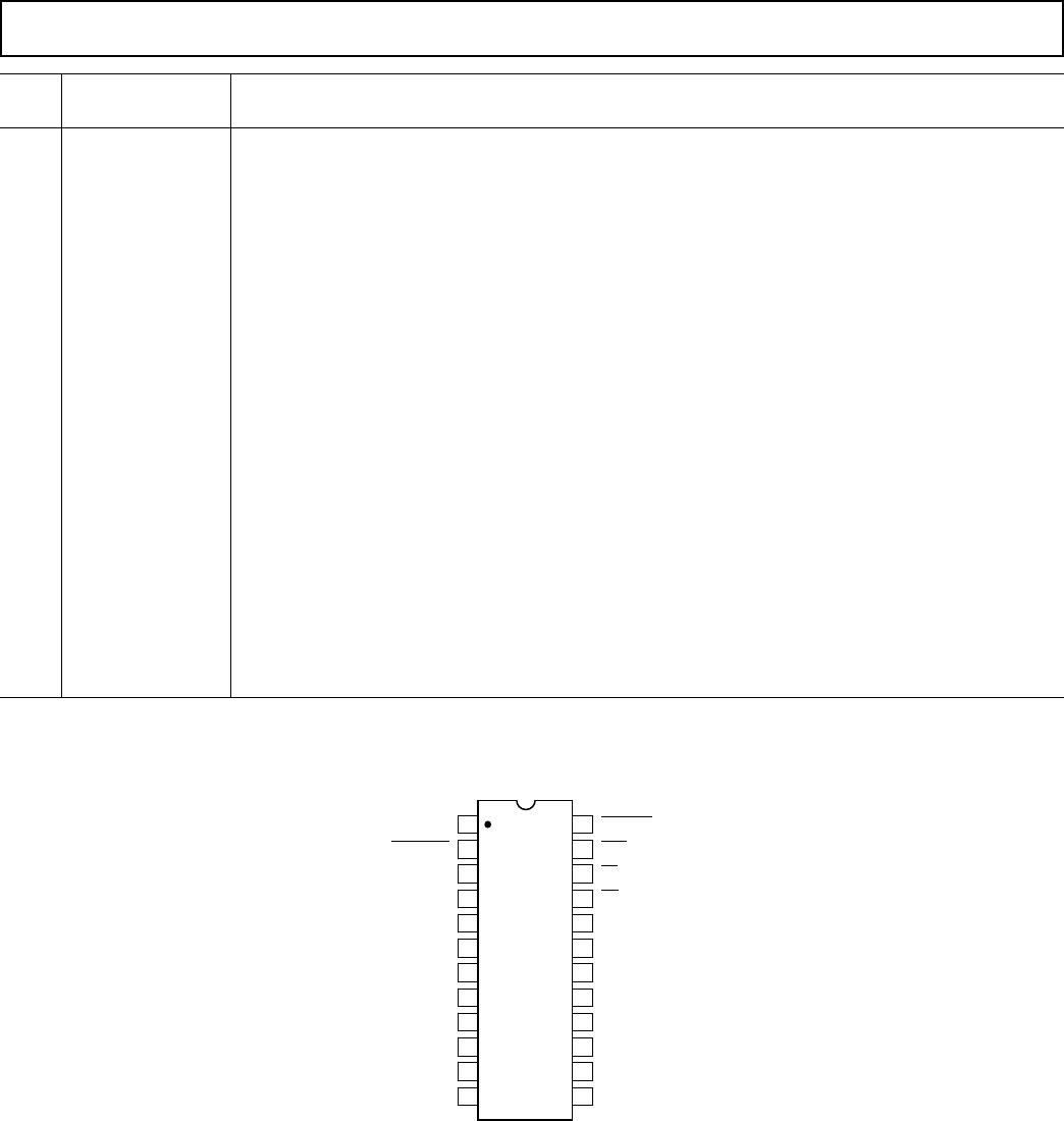
PIN CONFIGURATION
DIP and SOIC
V
DD
REF OUT/REF IN
AGND
MODE
DB0 (LSB)
DB1
DB2
V
IN2
V
IN1
DB11/LOW DB3/RFS
DB10/LOW
DB4/SCLK
DB9 DB5/SDATA
DB8
DGND
DB7 DB6
14
1
2
24
23
5
6
7
20
19
18
3
4
22
21
817
916
10 15
11
TOP VIEW
(Not to Scale)
11
12 13
AD7892
STANDBY
CONVST
EOC
CS
RD
AD7892
–8–
REV. C
Relative Accuracy
Relative accuracy or endpoint nonlinearity is the maximum
deviation from a straight line passing through the endpoints of
the ADC transfer function.
Differential Nonlinearity
This is the difference between the measured and the ideal
1 LSB change between any two adjacent codes in the ADC.
Positive Full-Scale Error (AD7892-1)
This is the deviation of the last code transition (01 . . . 110 to
01 . . . 111) from the ideal 4 × REF IN – 3/2 LSB (± 10 V range)
or 2 × REF IN – 3/2 LSB (± 5 V range) after the bipolar zero
error has been adjusted out.
Positive Full-Scale Error (AD7892-2)
This is the deviation of the last code transition (11 . . . 110 to
11 . . . 111) from the ideal (REF IN – 3/2 LSB) after the unipo-
lar offset error has been adjusted out.
Positive Full-Scale Error (AD7892-3)
This is the deviation of the last code transition (01 . . . 110 to
01 . . . 111) from the ideal (REF IN – 3/2 LSB) after the bipolar
zero error has been adjusted out.
Bipolar Zero Error (AD7892-1, AD7892-3)
This is the deviation of the midscale transition (all 1s to all 0s)
from the ideal (AGND – 1/2 LSB).
Unipolar Offset Error (AD7892-2)
This is the deviation of the first code transition (00 . . . 000 to
00 . . . 001) from the ideal (AGND + 1/2 LSB).
Negative Full-Scale Error (AD7892-1)
This is the deviation of the first code transition (10 . . . 000 to
10 . . . 001) from the ideal –4 × REF IN + 1/2 LSB (± 10 V
range) or –2 × REF IN + 1/2 LSB (±5 V range) after bipolar
zero error has been adjusted out.
Negative Full-Scale Error (AD7892-3)
This is the deviation of the first code transition (10 . . . 000 to
10 . . . 001) from the ideal – REF IN + 1/2 LSB after bipolar
zero error has been adjusted out.
Track/Hold Acquisition Time
Track/Hold acquisition time is the time required for the output
of the track/hold amplifier to reach its final value, within ± 1/2 LSB,
after the end of conversion (the point at which the track/hold
returns to track mode). It also applies to situations where there
is a step input change on the input voltage applied to the V
IN
input of the AD7892. It means that the user must wait for the
duration of the track/hold acquisition time after the end of con-
version or after a step input change to V
IN
before starting another
conversion, to ensure that the part operates to specification.
TERMINOLOGY
Signal to (Noise + Distortion) Ratio
This is the measured ratio of signal to (noise + distortion) at the
output of the A/D converter. The signal is the rms amplitude of
the fundamental. Noise is the rms sum of all nonfundamental
signals up to half the sampling frequency (f
S
/2), excluding dc.
The ratio is dependent upon the number of quantization levels
in the digitization process; the more levels, the smaller the quan-
tization noise. The theoretical signal to (noise + distortion)
ratio for an ideal N-bit converter with a sine wave input is given
by:
Signal to (Noise + Distortion) = (6.02 N + 1.76) dB
Thus for a 12-bit converter, this is 74 dB.
Total Harmonic Distortion
Total harmonic distortion (THD) is the ratio of the rms sum of
harmonics to the fundamental. For the AD7892, it is defined
as:
THD (dB) = 20 log
V
2
2
+V
3
2
+V
4
2
+V
5
2
+V
6
2
V
1
where V
1
is the rms amplitude of the fundamental and V
2
, V
3
,
V
4
, V
5
and V
6
are the rms amplitudes of the second through the
sixth harmonics.
Peak Harmonic or Spurious Noise
Peak harmonic or spurious noise is defined as the ratio of the
rms value of the next largest component in the ADC output
spectrum (up to f
S
/2 and excluding dc) to the rms value of the
fundamental. Normally, the value of this specification is deter-
mined by the largest harmonic in the spectrum, but for parts
where the harmonics are buried in the noise floor, it will be a
noise peak.
Intermodulation Distortion
With inputs consisting of sine waves at two frequencies, fa and
fb, any active device with nonlinearities will create distortion
products at sum and difference frequencies of mfa ± nfb where
m, n = 0, 1, 2, 3, etc. Intermodulation terms are those for
which neither m nor n are equal to zero. For example, the sec-
ond order terms include (fa + fb) and (fa – fb), while the third
order terms include (2fa + fb), (2fa – fb), (fa + 2fb) and
(fa – 2fb).
The AD7892 is tested using two input frequencies away from
the bottom end of the input bandwidth. In this case, the second
and third order terms are of different significance. The second
order terms are usually distanced in frequency from the original
sine waves while the third order terms are usually at a frequency
close to the input frequencies. As a result, the second and third
order terms are specified separately. The calculation of the
intermodulation distortion is as per the THD specification where it
is the ratio of the rms sum of the individual distortion products to
the rms amplitude of the fundamental expressed in dBs.

AD7892ANZ-1

Mfr. #:
Manufacturer:
Analog Devices Inc.
Description:
Analog to Digital Converters - ADC Bipolar Input Parallel 12B 600kSPS
Lifecycle:
New from this manufacturer.
Delivery:
DHL FedEx Ups TNT EMS
Payment:
T/T Paypal Visa MoneyGram Western Union