ADuM1240/ADuM1241/ADuM1245/ADuM1246 Data Sheet
Rev. B | Page 16 of 24
0
10
20
30
40
50
60
70
80
90
100
–40 –20 0 20 40 60 80 100 120 140
SUPPLY CURREN
T
PER CHANNEL
(
µA)
TEMPERATURE (°C)
OUTPUT
INPUT
11925-018
Figure 21. Typical Input and Output Supply Current per Channel vs.
Temperature for V
DDX
= 2.5 V, Data Rate = 1000 kbps
0
10
20
30
40
50
60
70
80
90
100
–40 –20 0 20 40 60 80 100 120 140
SUPPLY CURRENT PER CHANNEL (µA)
TEMPERATURE (°C)
OUTPUT
INPUT
11925-019
Figure 22. Typical Input and Output Supply Current per Channel vs.
Temperature for V
DDX
= 3.3 V, Data Rate = 1000 kbps
0
20
40
60
80
100
120
140
–40 –20 0 20 40 60 80 100 120 140
PROPAG
A
TION DEL
A
Y (ns)
TEMPERATURE (°C)
V
DDx
= 2.5V
V
DDx
= 3.3V
11925-020
Figure 23. Typical Propagation Delay vs. Temperature for
V
DDx
= 3.3 V or V
DDx
= 2.5 V
0
20
40
60
80
100
120
2.0 2.5 3.0 3.5 4.0
GLITCH FILTER WIDTH (ns)
TRANSMITTER V
DDx
(V)
11925-021
Figure 24. Typical Glitch Filter Operation Threshold
0
20
40
60
80
100
120
140
–40 –20 0 20 40 60 80 100 120 140
REFRESH PERIOD (µs)
TEMPERATURE (°C)
V
DDx
= 2.5V
V
DDx
= 3.3V
11925-022
Figure 25. Typical Refresh Period vs. Temperature for
3.3 V and 2.5 V Operation
0
20
40
60
80
100
120
2.0 2.5 3.0 3.5 4.0
REFRESH PERIOD (µs)
V
DDx
VOLTAGE (V)
11925-023
Figure 26. Typical Refresh Period vs. V
DDx
Voltage
Data Sheet ADuM1240/ADuM1241/ADuM1245/ADuM1246
Rev. B | Page 17 of 24
APPLICATIONS INFORMATION
PCB LAYOUT
The ADuM1240/ADuM1241/ADuM1245/ADuM1246 digital
isolators require no external interface circuitry for the logic
interfaces. Power supply bypassing is strongly recommended at
both the input and output supply pins: V
DD1
and V
DD2
(see
Figure 27). Maintain the capacitor value between 0.01 μF and
0.1 μF and for best results, ensure that the total lead length
between both ends of the capacitor and the input power supply
does not exceed 20 mm.
With proper PCB design choices, these digital isolators readily
meet CISPR 22 Class A (and FCC Class A) emissions standards,
as well as the more stringent CISPR 22 Class B (and FCC Class B)
standards in an unshielded environment. Refer to AN-1109 for
PCB related electromagnetic interference (EMI) mitigation
techniques, including board layout and stack up issues.
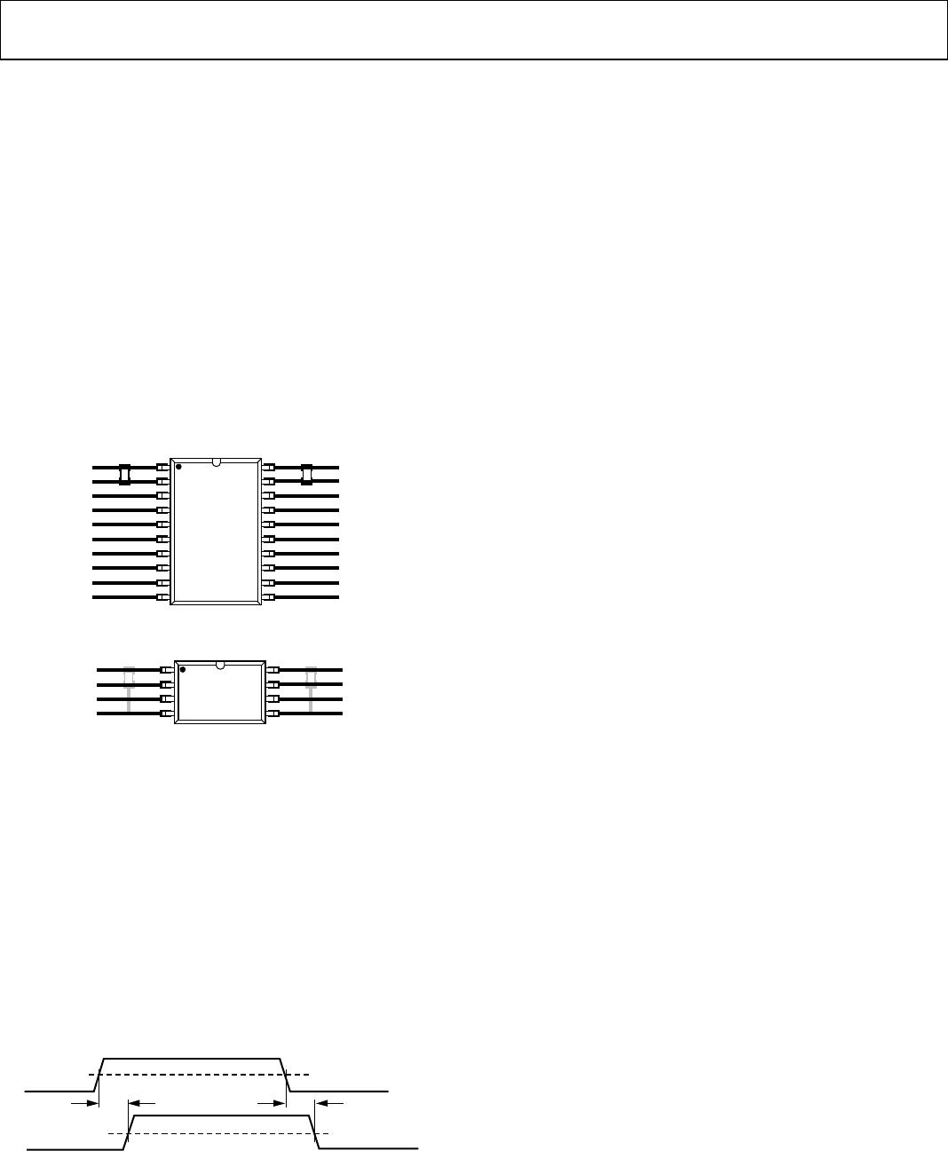
V
DD1
GND
1
NIC
NIC
V
IA/
V
OA
V
IB
EN
1
NIC
NIC = NOT INTERNALLY CONNECTED.
V
DD2
GND
2
NIC
NIC
V
OA/
V
IA
V
OB
EN
2
NIC
NIC
GND
1
NIC
GND
2
11925-024
Figure 27. Recommended PCB Layout, 20-Lead SSOP (RS-20)
V
DD1
V
IA/
V
OA
V
IB
V
DD2
V
OA/
V
IA
V
OB
GND
1
GND
2
11925-124
Figure 28. Recommended PCB Layout, 8-Lead SOIC (R-8)
For applications involving high common-mode transients, it is
important to minimize board coupling across the isolation barrier.
Furthermore, design the board layout so that any coupling that
does occur equally affects all pins on a given component side.
Failure to ensure this equal capacitive coupling of pins can
cause voltage differentials between pins exceeding the absolute
maximum ratings of the device, thereby leading to latch-up or
permanent damage.
PROPAGATION DELAY RELATED PARAMETERS
Propagation delay is a parameter that describes the time it takes
a logic signal to propagate through a component. The input to
output propagation delay time for a high to low transition can
differ from the propagation delay time of a low to high transition.
INPUT (V
Ix
)
OUTPUT (V
Ox
)
t
PLH
t
PHL
50%
50%
11925-025
Figure 29. Propagation Delay Parameters
Pulse width distortion is the maximum difference between
these two propagation delay values, and an indication of how
accurately the timing of the input signal is preserved.
Channel to channel matching refers to the maximum amount
the propagation delay differs between channels within a single
component of the ADuM1240/ADuM1241/ADuM1245/
ADuM1246.
Propagation delay skew refers to the maximum amount the
propagation delay differs between multiple ADuM1240/
ADuM1241/ADuM1245/ADuM1246 components operating
under the same conditions.
DC CORRECTNESS AND LOW POWER OPERATION
Standard Operating Mode
Positive and negative logic transitions at the isolator input cause
narrow (~1 ns) pulses to be sent to the decoder using the
transformer. The decoder is bistable and is, therefore, either set
or reset by the pulses, indicating input logic transitions. When
refresh and watchdog functions are enabled, by pulling EN
1
and
EN
2
low, in the absence of logic transitions at the input for more
than ~140 μs, a periodic set of refresh pulses, indicative of the
correct input state, is sent to ensure dc correctness at the output. If
the decoder receives no internal pulses of more than approximately
200 μs, the device assumes that the input side is unpowered or
nonfunctional, in which case, the isolator watchdog circuit
forces the output to a default state. The default state is either high,
as in the ADuM1240 and ADuM1241 versions, or low, as in the
ADuM1245 and ADuM1246 versions.
Low Power Operating Mode
For the lowest power consumption, disable the refresh and
watchdog functions of the ADuM1240/ADuM1241/ADuM1245/
ADuM1246 by pulling EN
1
and EN
2
to logic high. These control
pins must be set to the same value on each side of the component
for proper operation.
In this mode, the current consumption of the chip drops to the
microampere range. However, be careful when using this mode,
because dc correctness is no longer guaranteed at startup. For
example, if the following sequence of events occurs:
1. Power is applied to Side 1.
2. A high level is asserted on the V
IA
input.
3. Power is applied to Side 2.
The high on V
IA
is not automatically transferred to the Side 2
V
OA
, and there can be a level mismatch that is not corrected until a
transition occurs at V
IA
. When power is stable on each side, and a
transition occurs on the input of the channel, the input and output
state of that channel is correctly matched. This contingency can
be resolved in several ways, such as sending dummy data, or
toggling refresh on for a short period to force synchronization after
turn on.
ADuM1240/ADuM1241/ADuM1245/ADuM1246 Data Sheet
Rev. B | Page 18 of 24
Recommended Input Voltage for Low Power Operation
The ADuM1240/ADuM1241/ADuM1245/ADuM1246
implement Schmitt trigger input buffers so that the devices
operate cleanly in low data rate, or in noisy environments. Schmitt
triggers allow a small amount of shoot through current when the
input voltage is not approximate to either V
DDx
or GND
x
levels.
Shoot through is possible because the two transistors are both
slightly on when input voltages are in the middle of the supply
range. For many digital devices, this leakage is not a large portion
of the total supply current and cannot be noticed; however, in the
ultralow power
ADuM1240/ADuM1241/ADuM1245/ADuM1246, this leakage
can be larger than the total operating current of the device and
must not be ignored.
To achieve optimum power consumption with the ADuM1240/
ADuM1241/ADuM1245/ADuM1246, always drive the inputs as
near to V
DDx
or GND
x
levels as possible. Figure 17 and Figure 18
illustrate the shoot through leakage of an input; therefore, whereas
the logic thresholds of the input are standard CMOS levels,
optimum power performance is achieved when the input logic
levels are driven within 0.5 V of either V
DDx
or GND
x
levels.
MAGNETIC FIELD IMMUNITY
The limitation on the magnetic field immunity of the device is
set by the condition in which, induced voltage in the transformer
receiving coil is sufficiently large, to either falsely set or reset the
decoder. The following analysis defines such conditions. The
ADuM1240 is examined in a 3 V operating condition, because it
represents the typical mode of operation for these products.
The pulses at the transformer output have an amplitude greater
than 1.5 V. The decoder has a sensing threshold of about 1.0 V,
therefore establishing a 0.5 V margin in which induced voltages
are tolerated. The voltage induced across the receiving coil is
given by
V = (−dβ/dt)∑πr
n
2
; n = 1, 2, …, N
where:
β is the magnetic flux density.
r
n
is the radius of the n
th
turn in the receiving coil.
N is the number of turns in the receiving coil.
Given the geometry of the receiving coil in the ADuM1240, and
an imposed requirement that the induced voltage be, at most,
50% of the 0.5 V margin at the decoder, a maximum allowable
magnetic field is calculated as shown in Figure 30.
1000
1k
100M10k
MAXIMUM ALLOWABLE MAGNETIC FLUX (kgauss)
100k 1M
10M
MAGNETIC FIELD FREQUENCY (Hz)
100
10
1
0.1
0.01
0.001
1
1925-026
Figure 30. Maximum Allowable External Magnetic Flux Density
For example, at a magnetic field frequency of 1 MHz, the maxi-
mum allowable magnetic field of 0.5 kgauss induces a voltage of
0.25 V at the receiving coil. This is about 50% of the sensing
threshold and does not cause a faulty output transition. If such
an event occurs, with the worst case polarity, during a transmitted
pulse, it would reduce the received pulse from >1.0 V to 0.75 V.
This is still higher than the 0.5 V sensing threshold of the decoder.
The preceding magnetic flux density values correspond to specific
current magnitudes at given distances away from the ADuM1240
transformers. Figure 31 expresses these allowable current magni-
tudes as a function of frequency for selected distances. The
ADuM1240 is very insensitive to external fields. Only extremely
large, high frequency currents, very close to the component,
could potentially be a concern. For the 1 MHz example noted,
the user would have to place a 1.2 kA current 5 mm away from
the ADuM1240 to affect component operation.
1000
1k
100M10k
MAXIMUM ALLOWABLE CURRENT (kA)
100k 1M
10M
MAGNETIC FIELD FREQUENCY (Hz)
100
10
1
0.1
0.01
DISTANCE = 1m
DISTANCE = 100mm
DISTANCE = 5mm
11925-027
Figure 31. Maximum Allowable Current for
Various Currents to ADuM1240 Spacings
Note that at combinations of strong magnetic field and high
frequency, any loops formed by PCB traces could induce
sufficiently large error voltages to trigger the thresholds of
succeeding circuitry. Avoid PCB structures that form loops.

ADUM1240ARZ-RL7

Mfr. #:
Manufacturer:
Analog Devices Inc.
Description:
Digital Isolators DUAL-CHANNEL DI GITAL ISOLATORS
Lifecycle:
New from this manufacturer.
Delivery:
DHL FedEx Ups TNT EMS
Payment:
T/T Paypal Visa MoneyGram Western Union