Expand menu
Hello, Sign in
My Account
0
Cart
Home
Products
Sensors
Semiconductors
Passive Components
Connectors
Power
Electromechanical
Optoelectronics
Circuit Protection
Integrated Circuits - ICs
Main Products
Manufacturers
Blog
Services
About OMO
About Us
Contact Us
Check Stock
IRF8113TRPBF
P1-P3
P4-P6
P7-P9
P10-P10
IRF81
13PbF
4
www.irf.com
Fig 8.
Maximum Safe Operating Area
Fig 6.
Typical Gate Charge Vs.
Gate-to-Source Voltage
Fig 5.
Typical Capacitance Vs.
Drain-to-Source Voltage
Fig 7.
Typical Source-Drain Diode
Forward Voltage
1
10
100
V
DS
, D
rai
n-to-
Source V
olt
age (V
)
100
1000
10000
100000
C
,
C
a
p
a
c
i
t
a
n
c
e
(
p
F
)
Coss
Crss
Ciss
V
GS
= 0V, f = 1 MHZ
C
iss
= C
gs
+ C
gd
, C
ds
SHO
RTED
C
rss
= C
gd
C
oss
= C
ds
+ C
gd
0.2
0.4
0.6
0.8
1.0
1.2
V
SD
, Sou
rce
-toD
rain
Volta
ge
(V)
0.1
1.0
10.0
100.0
1000.0
I
S
D
,
R
e
v
e
r
s
e
D
r
a
i
n
C
u
r
r
e
n
t
(
A
)
T
J
= 25
°C
T
J
= 150°
C
V
GS
= 0V
0.1
1.0
10.0
100.0
1000.
0
V
DS
, D
rai
n-toS
ource V
oltage (
V)
0.1
1
10
100
1000
I
D
,
D
r
a
i
n
-
t
o
-
S
o
u
r
c
e
C
u
r
r
e
n
t
(
A
)
Tc =
25°C
Tj
= 150°
C
Si
ngle P
ulse
1msec
10msec
OPERATION IN THIS AREA
LIM
ITED BY R
DS
(on)
100µsec
0
1
02
03
04
0
5
06
0
Q
G
Tot
al G
ate Char
ge (nC)
0
2
4
6
8
10
12
V
G
S
,
G
a
t
e
-
t
o
-
S
o
u
r
c
e
V
o
l
t
a
g
e
(
V
)
V
DS
= 24
V
VDS= 15
V
I
D
= 13.
3A
IRF81
13PbF
www.irf.com
5
Fig 11.
Maximum Effective Transient Thermal Impedance, Junction-to-Ambient
Fig 9.
Maximum Drain Current Vs.
Case Temperature
Fig 10.
Threshold Voltage Vs. Temperature
1E-006
1E-005
0.0001
0.001
0.01
0.1
1
10
100
t
1
, R
ectangul
ar Pul
se Dur
ation (
sec)
0.001
0.01
0.1
1
10
100
T
h
e
r
m
a
l
R
e
s
p
o
n
s
e
(
Z
t
h
J
A
)
0.20
0.10
D = 0.50
0.02
0.01
0.05
SINGLE PUL
SE
( THERMAL RESPO
NSE )
Notes
:
1. Du
ty
Fac
tor
D = t1/t2
2. P
eak Tj
= P
dm x Zt
hja +
Tc
-75
-50
-25
0
25
50
75
100
125
150
T
J
, T
emperat
ure (
°C )
0.8
1.0
1.2
1.4
1.6
1.8
2.0
2.2
V
G
S
(
t
h
)
G
a
t
e
t
h
r
e
s
h
o
l
d
V
o
l
t
a
g
e
(
V
)
I
D
= 250µA
τ
J
τ
J
τ
1
τ
1
τ
2
τ
2
τ
3
τ
3
R
1
R
1
R
2
R
2
R
3
R
3
Ci=
i
/
Ri
Ci=
τ
i
/
Ri
τ
τ
C
τ
4
τ
4
R
4
R
4
Ri (°C/W)
τ
i (sec)
0.924 0.000228
13.395 0.1728
22.046 1.5543
14.911 22.5
25
50
75
100
125
150
T
J
, Junct
ion T
emperat
ure (°
C)
0
2
4
6
8
10
12
14
16
18
I
D
,
D
r
a
i
n
C
u
r
r
e
n
t
(
A
)
IRF81
13PbF
6
www.irf.com
D.U.T
.
V
D
S
I
D
I
G
3mA
V
GS
.3
µ
F
50K
Ω
.2
µ
F
12V
Current
Regulator
Same
Type
as
D.U.T
.
Current
Sampling
Resistors
+
-
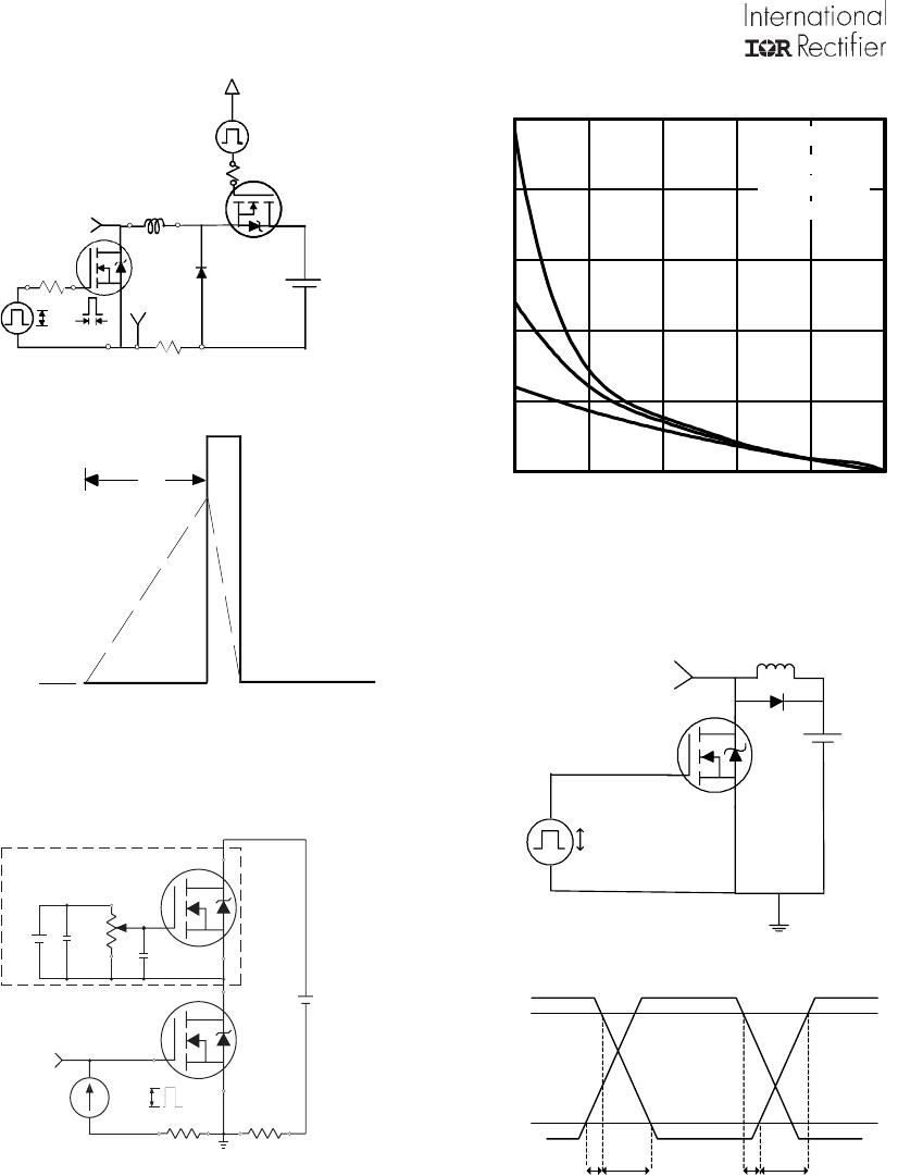
Fig 13.
Gate Charge Test Circuit
Fig 12b.
Unclamped Inductive Waveforms
Fig 12a.
Unclamped Inductive Test Circuit
t
p
V
(BR)DSS
I
AS
Fig 12c.
Maximum Avalanche Energy
Vs. Drain Current
R
G
I
AS
0.01
Ω
t
p
D.U.T
L
V
DS
+
-
V
DD
DRIVER
A
15V
20V
V
GS
25
50
75
100
125
150
St
art
ing T
J
, Junct
ion T
emperat
ure (°
C)
0
40
80
120
160
200
E
A
S
,
S
i
n
g
l
e
P
u
l
s
e
A
v
a
l
a
n
c
h
e
E
n
e
r
g
y
(
m
J
)
I
D
TOP
7.3
A
8.2
A
BOTTOM
13.3A
Fig 14a.
Switching Time Test Circuit
Fig 14b.
Switching Time Waveforms
V
GS
V
DS
9
0%
10%
t
d(
o
n)
t
d(off)
t
r
t
f
V
GS
Pu
lse
Widt
h < 1µs
Duty F
act
or < 0
.1%
V
DD
V
DS
L
D
D.U
.T
+
-
P1-P3
P4-P6
P7-P9
P10-P10
IRF8113TRPBF
Mfr. #:
Buy IRF8113TRPBF
Manufacturer:
Infineon / IR
Description:
MOSFET MOSFT 30V 16.6A 6mOhm 24nC
Lifecycle:
New from this manufacturer.
Delivery:
DHL
FedEx
Ups
TNT
EMS
Payment:
T/T
Paypal
Visa
MoneyGram
Western
Union
Products related to this Datasheet
IRF8113TRPBF
IRF8113PBF