IRF8113PbF
8 www.irf.com
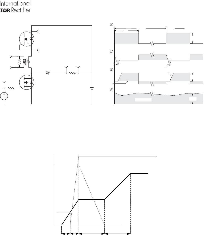
Control FET
Special attention has been given to the power losses
in the switching elements of the circuit - Q1 and Q2.
Power losses in the high side switch Q1, also called
the Control FET, are impacted by the R
ds(on)
of the
MOSFET, but these conduction losses are only about
one half of the total losses.
Power losses in the control switch Q1 are given
by;
P
loss
= P
conduction
+ P
switching
+ P
drive
+ P
output
This can be expanded and approximated by;
P
loss
= I
rms
2
× R
ds(on )
()
+ I ×
Q
gd
i
g
× V
in
× f
⎛
⎝
⎜
⎞
⎠
⎟
+ I ×
Q
gs2
i
g
× V
in
× f
⎛
⎝
⎜
⎞
⎠
⎟
+ Q
g
× V
g
× f
()
+
Q
oss
2
×V
in
× f
⎛
⎝
⎞
⎠
This simplified loss equation includes the terms Q
gs2
and Q
oss
which are new to Power MOSFET data sheets.
Q
gs2
is a sub element of traditional gate-source
charge that is included in all MOSFET data sheets.
The importance of splitting this gate-source charge
into two sub elements, Q
gs1
and Q
gs2
, can be seen from
Fig 16.
Q
gs2
indicates the charge that must be supplied by
the gate driver between the time that the threshold
voltage has been reached and the time the drain cur-
rent rises to I
dmax
at which time the drain voltage be-
gins to change. Minimizing Q
gs2
is a critical factor in
reducing switching losses in Q1.
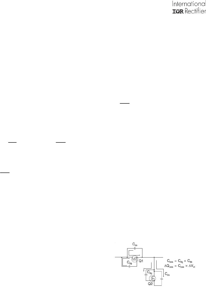
Q
oss
is the charge that must be supplied to the out-
put capacitance of the MOSFET during every switch-
ing cycle. Figure A shows how Q
oss
is formed by the
parallel combination of the voltage dependant (non-
linear) capacitances C
ds
and C
dg
when multiplied by
the power supply input buss voltage.
Synchronous FET
The power loss equation for Q2 is approximated
by;
loss
= P
conduction
+ P
drive
+ P
output
*
loss
= I
rms
2
× R
ds(on)()
+ Q
g
× V
g
× f
()
+
Q
oss
2
×V
in
× f
⎛
⎝
⎜
⎞
⎠
+ Q
rr
× V
in
×
(
*dissipated primarily in Q1.
For the synchronous MOSFET Q2, R
ds(on)
is an im-
portant characteristic; however, once again the im-
portance of gate charge must not be overlooked since
it impacts three critical areas. Under light load the
MOSFET must still be turned on and off by the con-
trol IC so the gate drive losses become much more
significant. Secondly, the output charge Q
oss
and re-
verse recovery charge Q
rr
both generate losses that
are transfered to Q1 and increase the dissipation in
that device. Thirdly, gate charge will impact the
MOSFETs’ susceptibility to Cdv/dt turn on.
The drain of Q2 is connected to the switching node
of the converter and therefore sees transitions be-
tween ground and V
in
. As Q1 turns on and off there is
a rate of change of drain voltage dV/dt which is ca-
pacitively coupled to the gate of Q2 and can induce
a voltage spike on the gate that is sufficient to turn
the MOSFET on, resulting in shoot-through current .
The ratio of Q
gd
/Q
gs1
must be minimized to reduce the
potential for Cdv/dt turn on.
Power MOSFET Selection for Non-Isolated DC/DC Converters
Figure A: Q
oss
Characteristic