LT5517EUF#PBF

LT5517
1
5517f
BPF
5V
V
CC
BPF
RF
+
RF
LPF
LT5517
I
OUT
+
I
OUT
0°
2xLO
ENENABLE
2xLO
INPUT
LPF
DSP
Q
OUT
+
Q
OUT
90°
÷2
5517 F01
LNA
VGA
VGA
Wireless Infrastructure
High Linearity Direct Conversion I/Q Receiver
High Linearity I/Q Demodulator
, LTC and LT are registered trademarks of Linear Technology Corporation.
RF Input Frequency Range: 40MHz to 900MHz
High IIP3: 21dBm at 800MHz
High IIP2: 58dBm at 800MHz
I/Q Gain Mismatch: 0.3dB Max
I/Q Phase Mismatch: 0.7°
Noise Figure: 12.4dB at 800MHz
Conversion Gain: 3.3dB at 800MHz
Baseband Bandwidth: 130MHz
Single Ended, 50 Matched 2XLO Input
Shutdown Mode
16-Lead QFN (4mm × 4mm) Package
with Exposed Pad
40MHz to 900MHz
Quadrature Demodulator
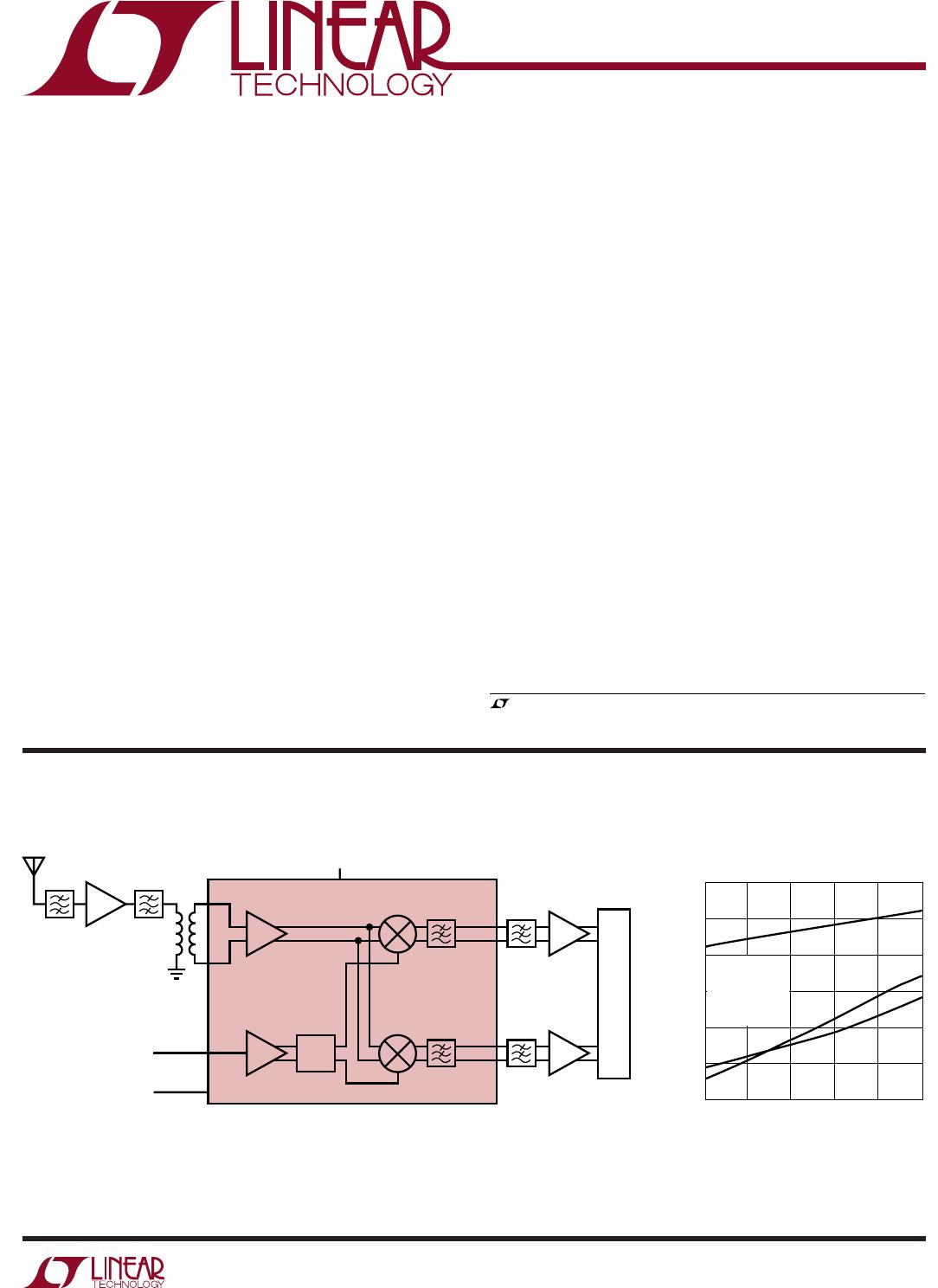
Figure 1. High Signal-Level I/Q Demodulator for 450MHz Infrastructure Receiver
I/Q Output Power, IM3, IM2
vs RF Input Power
The LT
®
5517 is a 40MHz to 900MHz quadrature demodu-
lator optimized for high linearity receiver applications
where high dynamic range is important. It is suitable for
communications receivers where an RF or IF signal is
directly converted into I and Q baseband signals with a
bandwidth up to 130MHz. The LT5517 incorporates bal-
anced I and Q mixers, LO buffer amplifiers and a precision,
broadband quadrature generator derived from an on-chip
divide-by-two circuit.
The superior linearity and low noise performance of the
LT5517 is achieved across its full frequency range. A well-
balanced divide-by-two circuit generates precision quadra-
ture LO carriers to drive the I mixer and the Q mixer.
Consequently, the outputs of the I-channel and the
Q-channel are well matched in amplitude, and their phases
are 90° apart. The LT5517 also provides excellent 50
impedance matching at the 2XLO port across its entire
frequency range.
RF INPUT POWER (dBm)
–18
–100
P
OUT
, IM3, IM2 (dBm/TONE)
–80
–60
–40
–20
0
20
P
OUT
IM3
IM2
–14 –10 –6 –2
5517 F01b
2
T
A
= 25°C
P
2XLO
= –10dBm
f
2XLO
= 1602MHz
f
RF1
= 799.9MHz
f
RF2
= 800.1MHz
FEATURES
DESCRIPTIO
U
APPLICATIO S
U
TYPICAL APPLICATIO
U
LT5517
2
5517f
Power Supply Voltage ............................................ 5.5V
Enable Voltage ....................................................0V, V
CC
2XLO Voltage (10dBm Equivalent) .......................... ±1V
RF
+
to RF
Differential Voltage
(10dBm Equivalent) ................................................. ±2V
Operating Ambient Temperature..............40°C to 85°C
Storage Temperature Range ................. 65°C to 125°C
Maximum Junction Temperature ..........................125°C
ORDER PART
NUMBER
Consult LTC Marketing for parts specified with wider operating temperature ranges.
LT5517EUF
ABSOLUTE AXI U RATI GS
W
WW
U
PACKAGE/ORDER I FOR ATIO
UUW
(Note 1)
T
A
= 25°C. V
CC
= 5V, EN = V
CC
, f
RF1
= 799.9MHz, f
RF2
= 800.1MHz,
f
2XLO
= 1602MHz, P
2XLO
= –10dBm, unless otherwise noted. (Notes 2, 3) (Test circuit shown in Figure 2)
PARAMETER CONDITIONS MIN TYP MAX UNITS
RF Frequency Range 40 to 900 MHz
2XLO Frequency Range 80 to 1800 MHz
2XLO Power 15 to 0 dBm
2XLO Port Return Loss Internally Matched to a 50 Source 20 dB
Conversion Gain Voltage Gain, Load Impedance = 1k 0 3.3 dB
Gain Variation vs Temperature –40°C to 85°C 0.01 dB/°C
Noise Figure 12.4 dB
Input 3rd Order Intercept 2-Tone, –10dBm/Tone, f = 200kHz 21 dBm
Input 2nd Order Intercept 2-Tone, –10dBm/Tone, f = 200kHz 58 dBm
Input 1dB Compression 10 dBm
Baseband Bandwidth 130 MHz
I/Q Gain Mismatch (Note 4) –0.3 0.03 0.3 dB
I/Q Phase Mismatch (Note 4) –3.5 0.7 3.5 deg
Output Impedance Differential 120
2XLO to RF Leakage 69 dBm
LO to RF Leakage 80 dBm
RF to 2XLO Isolation 63 dB
AC ELECTRICAL CHARACTERISTICS
T
JMAX
= 125°C, θ
JA
= 37°C/W
UF PART
MARKING
5517
16 15 14 13
5 6 7 8
TOP VIEW
UF PACKAGE
16-LEAD (4mm × 4mm) PLASTIC QFN
EXPOSED PAD (PIN 17) IS GND,
MUST BE SOLDERED TO PCB
9
10
11
12
4
3
2
1GNDRF
RF
+
RF
GNDRF
V
CC
GND
2XLO
GND
I
OUT
+
I
OUT
Q
OUT
+
Q
OUT
EN
V
CC
V
CC
V
CC
17
LT5517
3
5517f
DC ELECTRICAL CHARACTERISTICS
T
A
= 25°C. V
CC
= 5V unless otherwise noted.
PARAMETER CONDITIONS MIN TYP MAX UNITS
Supply Voltage 4.5 5.25 V
Supply Current 70 90 110 mA
Shutdown Current EN = LOW 0.1 20 µA
Turn-On Time (Note 5) 200 ns
Turn-Off Time (Note 5) 300 ns
EN = HIGH (On) 1.6 V
EN = LOW (Off) 1.3 V
EN Input Current V
ENABLE
= 5V 2 µA
Output DC Offset Voltage f
LO
= 1602MHz, P
LO
= –10dBm 0.5 30 mV
(
I
OUT
+
– I
OUT
, Q
OUT
+
– Q
OUT
)
Output DC Offset Variation vs Temperature 40°C to 85°C7µV/°C
Note 1: Absolute Maximum Ratings are those values beyond which the life
of a device may be impaired.
Note 2: Tests are performed as shown in the configuration of Figure 2.
Note 3: Specifications over the –40°C to 85°C temperature range are
assured by design, characterization and correlation with statistical process
control.
Note 4: Measured at P
2XLO
= –10dBm and output frequency = 1MHz.
Note 5: Turn ON and Turn OFF times are based on rise and fall times of the
output baseband voltage with RF input power of –10dBm.
TYPICAL PERFOR A CE CHARACTERISTICS
UW
Supply Current vs Supply Voltage
Conv Gain, NF, IIP3
vs RF Input Frequency
SUPPLY VOLTAGE (V)
4.5
SUPPLY CURRENT (mA)
80
90
5.5
5517 G01
70
60
4.75
5
5.25
110
100
T
A
= 85°C
T
A
= 25°C
T
A
= –40°C
RF INPUT FREQUENCY (MHz)
0
0
GAIN (dB), NF (dB), IIP3 (dBm)
5
15
20
25
200
400
500 900
5517 G02
10
100 300
600
700
800
IIP3
NF
CONV GAIN
P
2XLO
= –10dBm
V
CC
= 5V
T
A
= 25°C
RF INPUT FREQUENCY (MHz)
0
30
IIP2 (dBm)
40
60
70
80
200
400
500 900
5517 G03
50
100 300
600
700
800
P
2XLO
= –10dBm
V
CC
= 5V
T
A
= 25°C
IIP2 vs RF Input Frequency
f
RF
= 800MHz, P
2XLO
= –10dBm, unless otherwise noted. (Test circuit shown in Figure 2)

LT5517EUF#PBF

Mfr. #:
Manufacturer:
Analog Devices Inc.
Description:
Modulator / Demodulator 40MHz - 900MHz Quadrature Demodulator
Lifecycle:
New from this manufacturer.
Delivery:
DHL FedEx Ups TNT EMS
Payment:
T/T Paypal Visa MoneyGram Western Union

Products related to this Datasheet