
LT5517EUF#PBF

LT5517
10
5517f
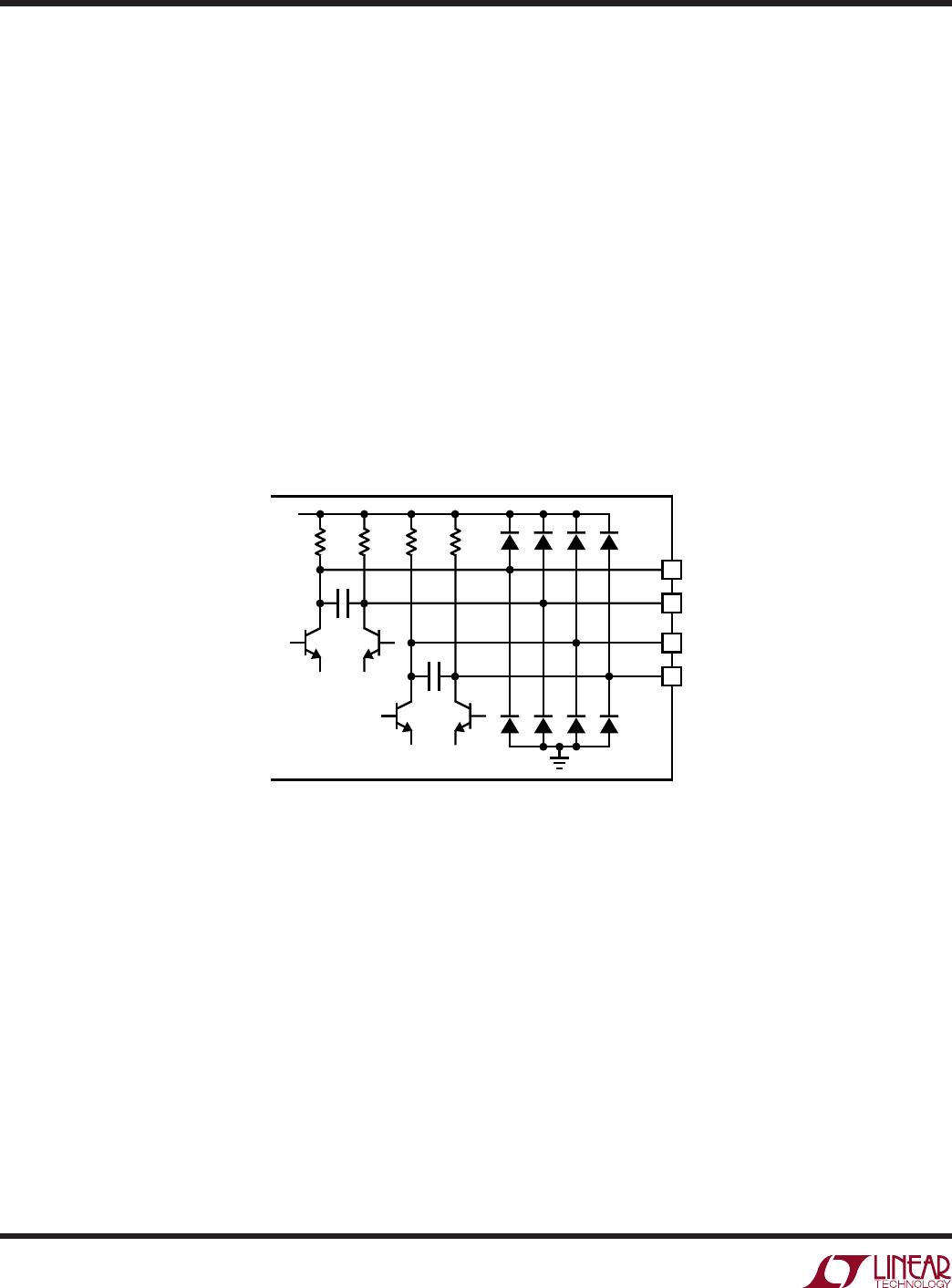
Figure 7. I/Q Output Equivalent Circuit
APPLICATIO S I FOR ATIO
WUUU
15
16
V
CC
10pF
I
OUT
+
I
OUT
5517 F07
13
14
10pF
Q
OUT
+
Q
OUT
60 60 60 60
approach is to terminate each output with a shunt capaci-
tor. The capacitor value can be optimized depending upon
the operating frequency and the specific PCB layout.
The phase relationship between the I-channel output sig-
nal and the Q-channel output signal is fixed. When the LO
input frequency is higher than the RF input frequency, then
the Q-channel outputs (Q
OUT
+
, Q
OUT
) lead the I-channel
outputs (I
OUT
+
, I
OUT
) by 90°.
When the LO input frequency is lower than the RF input
frequency, then the Q-channel outputs lag the I-channel
outputs by 90°. Note that the phase relationship of the I-
and Q-channel outputs relative to the LO can vary by 180°,
depending on start-up conditions. This is the nature of a
frequency divider-based quadrature phase generator.
When AC output coupling is used, the resulting highpass
filter’s –3dB roll-off frequency is defined by the R-C
constant of the blocking capacitor and R
LOAD
, assuming
R
LOAD
> 600.
Care should be taken when the demodulator’s outputs are
DC coupled to the external load to make sure that the I/Q
mixers are biased properly. If the current drain from the
outputs exceeds 6mA, there can be significant degrada-
tion of the linearity performance. Each output can sink no
more than 13mA when connected to an external load with
a DC voltage higher than V
CC
– 0.78V.
LT5517
11
5517f
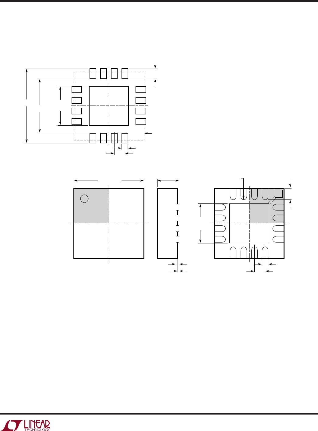
UF Package
16-Lead Plastic QFN (4mm × 4mm)
(Reference LTC DWG # 05-08-1692)
U
PACKAGE DESCRIPTIO
4.00 ± 0.10
(4 SIDES)
NOTE:
1. DRAWING CONFORMS TO JEDEC PACKAGE OUTLINE MO-220 VARIATION (WGGC)
2. ALL DIMENSIONS ARE IN MILLIMETERS
3. DIMENSIONS OF EXPOSED PAD ON BOTTOM OF PACKAGE DO NOT INCLUDE
MOLD FLASH. MOLD FLASH, IF PRESENT, SHALL NOT EXCEED 0.15mm ON ANY SIDE
4. EXPOSED PAD SHALL BE SOLDER PLATED
PIN 1
TOP MARK
0.55 ± 0.20
1615
1
2
BOTTOM VIEW—EXPOSED PAD
2.15 ± 0.10
(4-SIDES)
0.75 ± 0.05
R = 0.115
TYP
0.30 ± 0.05
0.65 BSC
0.200 REF
0.00 – 0.05
(UF) QFN 0503
RECOMMENDED SOLDER PAD PITCH AND DIMENSIONS
0.72 ±0.05
0.30 ±0.05
0.65 BSC
2.15 ± 0.05
(4 SIDES)
2.90 ± 0.05
4.35 ± 0.05
PACKAGE OUTLINE
Information furnished by Linear Technology Corporation is believed to be accurate and reliable.
However, no responsibility is assumed for its use. Linear Technology Corporation makes no represen-
tation that the interconnection of its circuits as described herein will not infringe on existing patent rights.
LT5517
12
5517f
Linear Technology Corporation
1630 McCarthy Blvd., Milpitas, CA 95035-7417
(408) 432-1900
FAX: (408) 434-0507
www.linear.com
LINEAR TECHNOLOGY CORPORATION 2004
LT/TP 0104 1K • PRINTED IN USA
RELATED PARTS
PART NUMBER DESCRIPTION COMMENTS
Infrastructure
LT5511 High Linearity Upconverting Mixer RF Output to 3GHz, 17dBm IIP3, Integrated LO Buffer
LT5512 DC-3GHz High Signal Level Downconverting Mixer DC to 3GHz, 21dBm IIP3, Integrated LO Buffer
LT5515 1.5GHz to 2.5GHz Direct Conversion Quadrature Demodulator 20dBm IIP3, Integrated LO Quadrature Generator
LT5516 0.8GHz to 1.5GHz Direct Conversion Quadrature Demodulator 21.5dBm IIP3, Integrated LO Quadrature Generator
LT5520 1.3GHz to 2.3GHz High Linearity Upconverting Mixer 15.9dBm IIP3, Single Ended, 50 Matched RF and LO Ports
LT5522 600MHz to 2.7GHz High Signal Level Downconverting Mixer 4.5V to 5.25V Supply, 25dBm IIP3 at 900MHz, NF = 12.5dB,
50 Single-Ended RF and LO Ports
RF Power Detectors
LT5504 800MHz to 2.7GHz RF Measuring Receiver 80dB Dynamic Range, Temperature Compensated,
2.7V to 5.25V Supply
LTC
®
5505 RF Power Detectors with >40dB Dynamic Range 300MHz to 3GHz, Temperature Compensated, 2.7V to 6V Supply
LTC5507 100kHz to 1000MHz RF Power Detector 100kHz to 1GHz, Temperature Compensated, 2.7V to 6V Supply
LTC5508 300MHz to 7GHz RF Power Detector 44dB Dynamic Range, Temperature Compensated, SC70 Package
LTC5509 300MHz to 3GHz RF Power Detector 36dB Dynamic Range, Low Power Consumption, SC70 Package
LTC5532 300MHz to 7GHz Precision RF Power Detector Precision V
OUT
Offset Control, Adjustable Gain and Offset
RF Building Blocks
LT5500 1.8GHz to 2.7GHz Receiver Front End 1.8V to 5.25V Supply, Dual-Gain LNA, Mixer, LO Buffer
LT5502 400MHz Quadrature IF Demodulator with RSSI 1.8V to 5.25V Supply, 70MHz to 400MHz IF, 84dB Limiting Gain,
90dB RSSI Range
LT5503 1.2GHz to 2.7GHz Direct IQ Modulator and 1.8V to 5.25V Supply, Four-Step RF Power Control,
Upconverting Mixer 120MHz Modulation Bandwidth
LT5506 500MHz Quadrature IF Demodulator with VGA 1.8V to 5.25V Supply, 40MHz to 500MHz IF, –4dB to 57dB
Linear Power Gain, 8.8MHz Baseband Bandwidth
LT5546 500MHz Ouadrature IF Demodulator with 17MHz Baseband Bandwidth, 40MHz to 500MHz IF, 1.8V to 5.25V
VGA and 17MHz Baseband Bandwidth Supply, –7dB to 56dB Linear Power Gain
RF Power Controllers
LTC1757A RF Power Controller Multiband GSM/DCS/GPRS Mobile Phones
LTC1758 RF Power Controller Multiband GSM/DCS/GPRS Mobile Phones
LTC1957 RF Power Controller Multiband GSM/DCS/GPRS Mobile Phones
LTC4400 SOT-23 RF PA Controller Multiband GSM/DCS/GPRS Phones, 45dB Dynamic Range,
450kHz Loop BW
LTC4401 SOT-23 RF PA Controller Multiband GSM/DCS/GPRS Phones, 45dB Dynamic Range,
250kHz Loop BW
LTC4403 RF Power Controller for EDGE/TDMA Multiband GSM/GPRS/EDGE Mobile Phones
LT5517EUF#PBF

Mfr. #:
Manufacturer:
Analog Devices Inc.
Description:
Modulator / Demodulator 40MHz - 900MHz Quadrature Demodulator
Lifecycle:
New from this manufacturer.
Delivery:
DHL FedEx Ups TNT EMS
Payment:
T/T Paypal Visa MoneyGram Western Union

Products related to this Datasheet