LT5517EUF#PBF

LT5517
7
5517f
Figure 2. Evaluation Circuit Schematic
Figure 4. Component Side Layout of Evaluation BoardFigure 3. Component Side Silkscreen of Evaluation Board
TEST CIRCUIT
I
OUT
J3
I
OUT
+
J4
RF
J1
Q
OUT
+
J5
Q
OUT
J6
C10
3.3pF
R2
0
C11
1nF
C12
1nF
J2
2XLO
C5
1nF
EN
5678
16 15 14 13
17
R1
100k
C3
0.1µF
C4
2.2µF
V
CC
LT5517
GNDRF
RF
+
RF
GNDRF
V
CC
GND
2XLO
GND
1
2
3
4
12
11
10
9
I
OUT
+
I
OUT
Q
OUT
+
Q
OUT
EN
V
CC
V
CC
V
CC
REFERENCE
DESIGNATION VALUE SIZE PART NUMBER
C1,C2,C5,C11,C12 1nF 0603 AVX 06033A102JAT1A
C3 0.1µF 0603 TAIYO YUDEN EMK107B
C4 2.2µF 0603 TAIYO YUDEN JMK107B
C10 3.3pF 0603 AVX 06033A3R3KAT2A
C13 TO C16 10pF 0805 AVX 08055A100ZAT1A
R1 100k 0603 OPTIONAL
R2 0 0603 JUMPER, OPTIONAL
T1 1:4 M/A COM MABAES0054
5517 F02
C15
10pF
C16
10pF
C1
1nF
T1
MABAES0054
C2
1nF
C13
10pF
C14
10pF
LT5517
8
5517f
APPLICATIO S I FOR ATIO
WUUU
The LT5517 is a direct I/Q demodulator targeting high
linearity receiver applications. It consists of an RF ampli-
fier, I/Q mixers, a quadrature LO carrier generator and bias
circuitry.
The RF signal is applied to the inputs of the RF amplifier,
and is then demodulated into I-channel and Q-channel
baseband signals using precision quadrature LO signals,
which are internally generated using a divide-by-two cir-
cuit. The demodulated I/Q signals are lowpass filtered
internally with a –3dB bandwidth of 130MHz. The differen-
tial outputs of the I-channel and Q-channel are well matched
in amplitude and their phases are 90° apart across the full
frequency range from 40MHz to 900MHz.
RF Input Port
Differential drive is recommended for the RF inputs as
shown in Figure 2. A low loss 1:4 transformer is used on
the demonstration board for a wide bandwidth input
impedance match and to assure good noise figure and
maximum demodulator gain. Single-ended to differential
conversion can also be implemented using narrowband
L-C circuits to produce the required balanced waveforms
at the RF
+
and RF
inputs using three discrete elements as
shown in Figure 5. Nominal values are listed in Table 1. (In
practice, these values should be compensated according
to the parasitics of the PCB.) The conversion gain and NF
of the receiver are similar to those of the transformer-
coupled demo board, because the single-ended to differ-
ential conversion has a 1:4 impedance transformation,
similar to the transformer.
Table 1. The Component Values of Matching Network L
SH
, C
S1
and C
S2
FREQUENCY (MHz) L
SH
(nH) C
S1
, C
S2
(pF)
40 437 71.1
100 169 28.6
200 80.8 14.3
300 51.5 9.6
400 37 7.2
500 28.3 5.8
600 22.6 4.9
700 18.5 4.2
800 15.6 3.7
900 13.5 3.3
The differential impedance of the RF inputs is listed in
Table 2. The RF inputs may also be terminated in a single-
ended configuration. In this case either the RF
+
or the RF
input can be simply AC coupled to a 50 source, while the
other RF input is connected to ground with a 1nF capacitor.
Note, however, that this will result in degraded conversion
gain and noise figure in most cases.
Figure 5. RF Input Matching Network at 800MHz
L
SH
15.6nH
TO RF
+
TO RF
MATCHING NETWORK
C
S1
3.7pF
RF
INPUT
5517 F05
C
S2
3.7pF
LT5517
9
5517f
Table 2. RF Input Differential Impedance
FREQUENCY DIFFERENTIAL INPUT
DIFFERENTIAL S11
(MHz) IMPEDANCE () MAG ANGLE(°)
40 240.1-j10.3 0.665 0.8
100 245.5-j25.9 0.664 2.5
200 236.8-j50.0 0.664 5.1
300 223.6-j70.5 0.663 –7.6
400 207.9-j86.3 0.662 10.2
500 190.6-j98.1 0.660 12.7
600 173.2-j105.8 0.657 15.3
700 156.2-j110.2 0.655 17.9
800 141.2-j111.8 0.651 20.4
900 129.5-j114.5 0.650 22.9
2XLO Input Port
To ease the interface of the receiver with the external 2XLO
input, the 2XLO port is designed with on-chip 50 imped-
ance matching up to 2GHz. The input is internally biased
at 1V. A 1nF DC blocking capacitor is required when
connected to the external 2XLO source.
The 2XLO frequency is required to be twice the desired
operating frequency in order for the chip to generate the
APPLICATIO S I FOR ATIO
WUUU
quadrature Local Oscillator (LO) signals for the demodu-
lator. The on-chip divide-by-two circuit delivers well-
matched, quadrature LO carriers to the I mixer and the Q
mixer.
I-Channel and Q-Channel Outputs
Each of the I-channel and Q-channel outputs is internally
connected to V
CC
though a 60 resistor. The output DC
bias voltage is V
CC
– 0.78V. The outputs can be DC coupled
or AC coupled to the external loads. The differential output
impedance of the demodulator is 120 in parallel with a
10pF internal capacitor, forming a lowpass filter with a
3dB corner frequency at 130MHz. The load impedance,
R
LOAD
, should be larger than 600 to assure full gain. The
gain is reduced by 20 • log(1 + 120/R
LOAD
) in dB when
the differential output is terminated by R
LOAD
. For ex-
ample, the gain is reduced by 6.85dB when each output pin
is connected to a 50 load (or 100 differential loads).
The output should be taken differentially (or by using
differential-to-single-ended conversion) for best RF per-
formance, including NF and IM2. Proper filtering of the
unwanted high frequency mixing product is also impor-
tant to maintain the highest linearity. A convenient
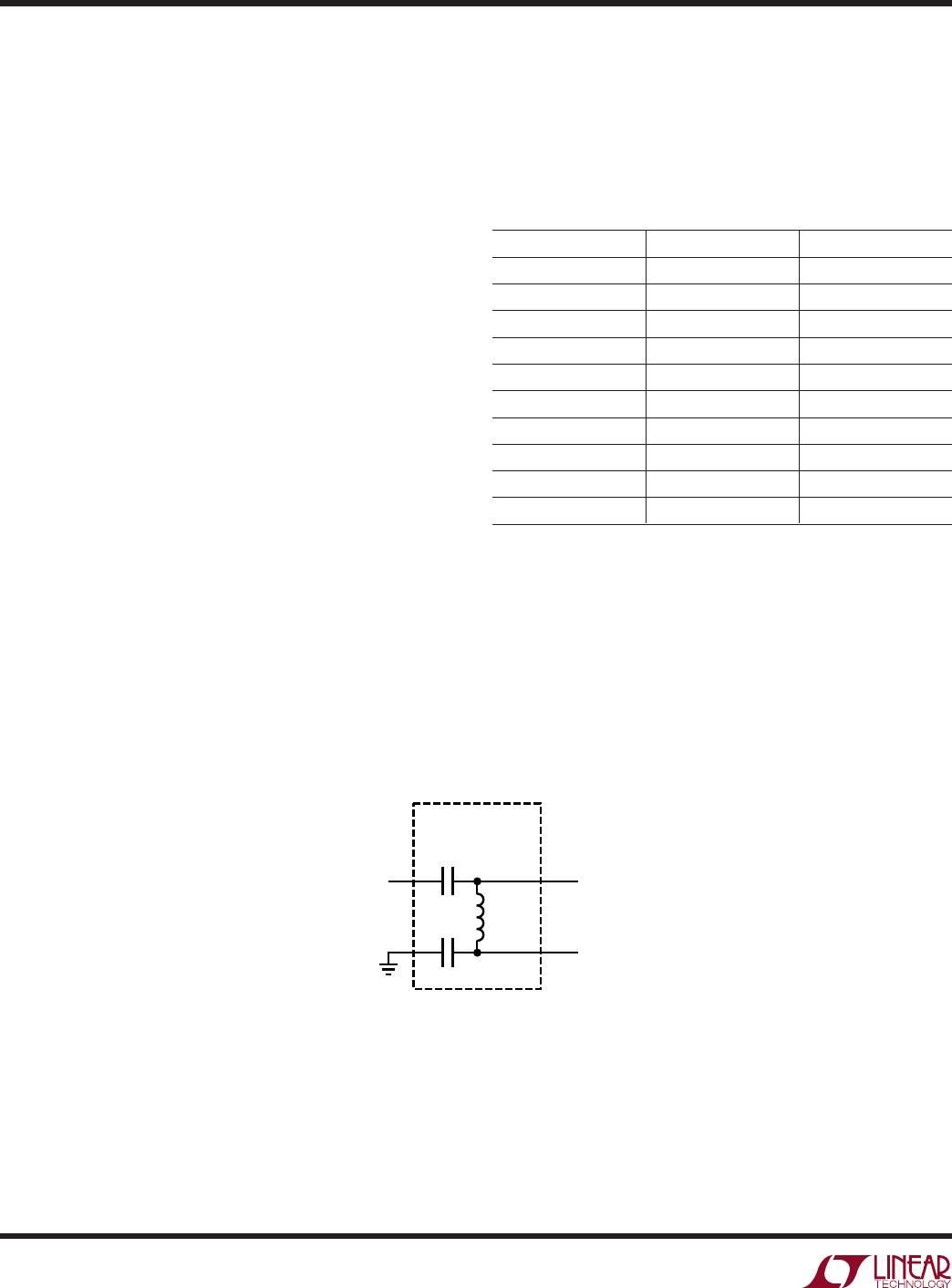
Figure 6. RF Input Equivalent Circuit with External Broadband Matching
3
2
V
CC
LT5517
RF
+
1
2
3
5
4
RF
5517 F06
250
2.30V
RF
J1
C10
3.3pF
C1
1nF
T1
MABAES0054
C2
1nF

LT5517EUF#PBF

Mfr. #:
Manufacturer:
Analog Devices Inc.
Description:
Modulator / Demodulator 40MHz - 900MHz Quadrature Demodulator
Lifecycle:
New from this manufacturer.
Delivery:
DHL FedEx Ups TNT EMS
Payment:
T/T Paypal Visa MoneyGram Western Union

Products related to this Datasheet