LT5517
5
5517f
UU
U
PI FU CTIO S
GNDRF (Pins 1, 4): Ground Pins for RF Termination.
These pins are not internally connected, and should be
connected to the PCB ground plane for best RF isolation.
RF
+
, RF
–
(Pins 2, 3): Differential RF Input Pins. These pins
are internally biased to 2.30V. These two pins should be
DC blocked when connected to ground or other matching
components. The inputs can be terminated in a single-
ended configuration, but differential input drive is pre-
ferred for best performance. An external matching network
is required for impedance transformation.
EN (Pin 5): Enable Pin. When the input voltage is higher
than 1.6V, the circuit is completely turned on. When the
input voltage is less than 1.3V, the circuit is turned off.
V
CC
(Pins 6, 7, 8, 12): Power Supply Pins. These pins
should be decoupled using 1000pF and 0.1µF capacitors.
GND (Pins 9, 11): Ground Pins. These pins are internally
tied together and to the Exposed Pad. They should be
connected to the PCB ground plane.
2XLO (Pin 10): 2XLO Input Pin. This pin is internally
biased to 1V. The input signal’s frequency should be twice
that of the desired demodulator LO frequency. The pin
should be AC coupled with an external DC blocking
capacitor.
Q
OUT
–
, Q
OUT
+
(Pins 13, 14): Differential Baseband Output
Pins of the Q-Channel. The internal DC bias voltage is
V
CC
– 0.78V for each pin.
I
OUT
–
, I
OUT
+
(Pins 15, 16): Differential Baseband Output
Pins of the I-Channel. The internal DC bias voltage is
V
CC
– 0.78V for each pin.
Exposed Pad (Pin 17): Ground Return for the Entire IC.
This pin must be soldered to the printed circuit board
ground plane.
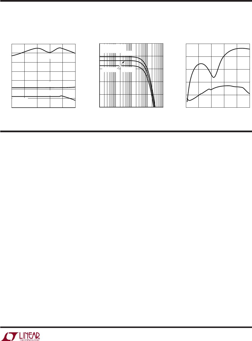
RF-LO Isolation
vs RF Input Power
Conv Gain
vs Baseband Frequency
RF, 2XLO Port Return Loss
vs Frequency
RF INPUT POWER (dBm)
–15
100
110
120
5
5517 G13
90
80
–10 –5 0 10
70
60
50
RF-LO ISOLATION (dB)
f
RF
= 800MHz
f
RF
= 400MHz
f
RF
= 40MHz
T
A
= 25°C
V
CC
= 5V
BASEBAND FREQUENCY (MHz)
–2
CONV GAIN (dB)
0
2
4
6
0.1 10 100 1000
5517 G14
–4
1
T
A
= 85°C
f
2XLO
= 1602MHz
V
CC
= 5V
T
A
= –40°C
T
A
= 25°C
FREQUENCY (GHz)
0
RETURN LOSS (dB)
–10
–5
0
1.60
5517 G15
–15
RF
LO
–20
–25
0.40
0.80
1.20
2
TYPICAL PERFOR A CE CHARACTERISTICS
UW
f
RF
= 800MHz, P
2XLO
= –10dBm, unless otherwise noted. (Test circuit shown in Figure 2)