LTC2450-1
10
24501fc
APPLICATIONS INFORMATION
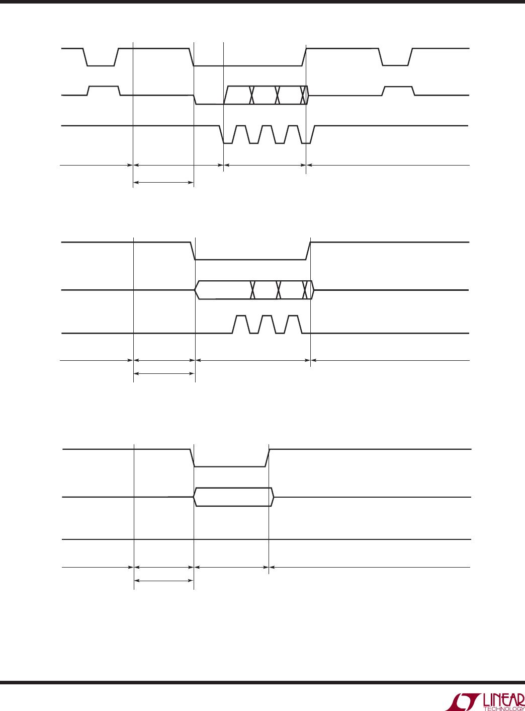
Serial Clock Idle-High (CPOL = 1) Examples
In Figure 5, following a conversion cycle the LTC2450-1
automatically enters the low power sleep mode. The user
can monitor the conversion status at convenient intervals
using CS and SDO.
CS is pulled LOW while SCK is HIGH to test whether or not
the chip is in the CONVERT state. While in the CONVERT
state, SDO is HIGH while CS is LOW. In the SLEEP state,
SDO is LOW while CS is LOW. These tests are not required
operational steps but may be useful for some applications.
When the data is available, the user applies 16 clock cycles
to transfer the result. The CS rising edge is then used to
initiate a new conversion.
The operation example of Figure 6 is identical to that of
Figure 5, except the new conversion cycle is triggered by
the falling edge of the serial clock (SCK). A 17th clock
pulse is used to trigger a new conversion cycle.
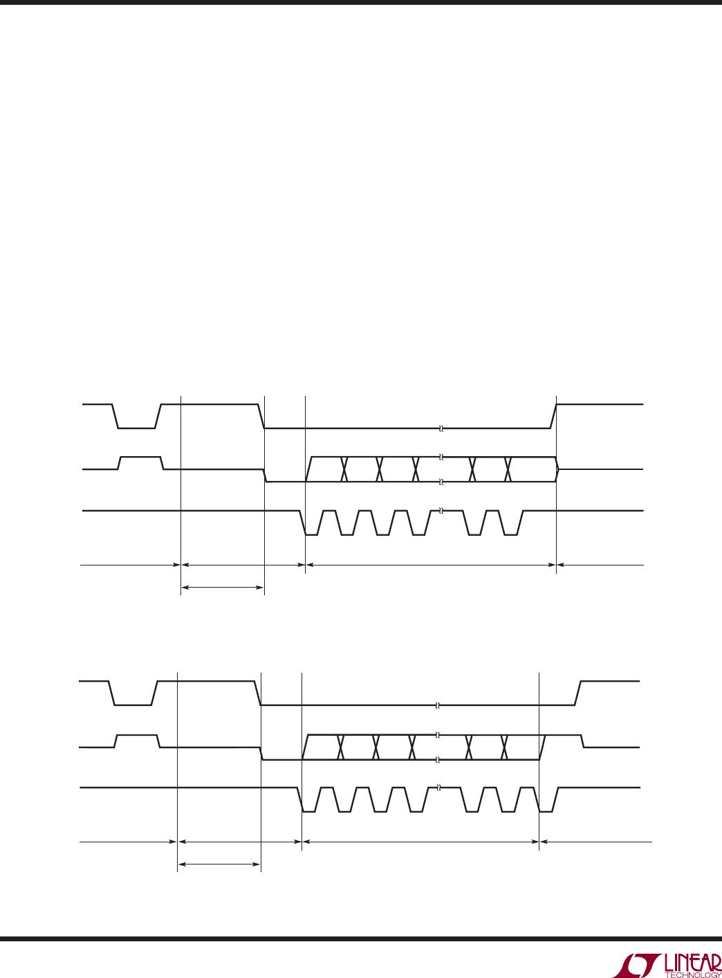
Serial Clock Idle-Low (CPOL = 0) Examples
In Figure 7, following a conversion cycle the LTC2450-1
automatically enters the low power sleep state. The user
determines data availability (and the end of conversion)
based upon external timing. The user then pulls CS low
(CS = ↓) and uses 16 clock cycles to transfer the result.
Following the 16th rising edge of the clock, CS is pulled high
(CS = ), which triggers a new conversion.
The timing diagram in Figure 8 is identical to that of Figure 7,
except in this case a new conversion is triggered by SCK.
The 16th SCK falling edge triggers a new conversion cycle
and the CS signal is subsequently pulled high.
Figure 5. Idle-High (CPOL = 1) Serial Clock Operation Example.
The Rising Edge of CS Starts a New Conversion
Figure 6. Idle-High (CPOL = 1) Clock Operation Example.
A 17th Clock Pulse is Used to Trigger a New Conversion Cycle
D
15
clk
1
clk
2
clk
3
clk
4
clk
15
clk
16
D
14
D
13
D
12
D
2
D
1
D
0
SD0
SCK
CONVERT CONVERTSLEEP
LOW I
CC
DATA OUTPUT
24501 F05
CS
D
15
D
14
D
13
D
12
D
2
D
1
D
0
SD0
clk
1
clk
2
clk
3
clk
4
clk
15
clk
16
clk
17
SCK
CONVERT CONVERTSLEEP
LOW I
CC
DATA OUTPUT
24501 F06
CS
LTC2450-1
11
24501fc
Examples of Aborting Cycle using CS
For some applications the user may wish to abort the I/O
cycle and begin a new conversion. If the LTC2450-1 is in
the data output state, a CS rising edge clears the remaining
data bits from memory, aborts the output cycle and triggers
a new conversion. Figure 9 shows an example of aborting
an I/O with idle-high (CPOL = 1) and Figure 10 shows an
example of aborting an I/O with idle-low (CPOL = 0).
A new conversion cycle can be triggered using the CS
signal without having to generate any serial clock pulses
as shown in Figure 11. If SCK is maintained at a LOW
logic level, after the end of a conversion cycle, a new
conversion operation can be triggered by pulling CS low
and then high. When CS is pulled low (CS = LOW), SDO
will output the most signifi cant bit (D15) of the result of
the just completed conversion. While a low logic level is
maintained at SCK pin and CS is subsequently pulled high
(CS = HIGH) the remaining 15 bits of the result (D14:D0)
are discarded and a new conversion cycle starts.
Following the aborted I/O, additional clock pulses in the
CONVERT state are acceptable, but excessive signal tran-
sitions on SCK can potentially create noise on the ADC
during the conversion, and thus may negatively infl uence
the conversion accuracy.
APPLICATIONS INFORMATION
Figure 8. Idle-Low (CPOL = 0) Clock. The 16th SCK Falling Edge Triggers a New Conversion
Figure 7. Idle-Low (CPOL = 0) Clock. CS Triggers a New Conversion
D
15
D
14
D
13
D
12
D
2
D
1
D
0
clk
1
clk
2
clk
3
clk
4
clk
14
clk
15
clk
16
SCK
SD0
CONVERT CONVERTSLEEP
LOW I
CC
DATA OUTPUT
24501 F07
CS
D
15
D
14
D
13
D
12
D
2
D
1
D
0
SD0
clk
1
clk
2
clk
3
clk
4
clk
15
clk
14
clk
16
SCK
CONVERT CONVERTSLEEP
LOW I
CC
DATA OUTPUT
24501 F08
CS
LTC2450-1
12
24501fc
D
15
D
14
D
13
clk
1
clk
2
clk
4
clk
3
CONVERT CONVERTSLEEP
LOW I
CC
DATA OUTPUT
24501 F09
SD0
SCK
CS
Figure 9. Idle-High (CPOL = 1) Clock and Aborted I/O Example
APPLICATIONS INFORMATION
D
15
D
14
D
13
SD0
clk
1
clk
2
clk
3
SCK
CONVERT CONVERTSLEEP
LOW I
CC
DATA OUTPUT
24501 F10
CS
Figure 10. Idle-Low (CPOL = 0) Clock and Aborted I/O Example
SCK = LOW
SD0
CONVERT CONVERTSLEEP
LOW I
CC
DATA OUTPUT
24501 F11
D
15
CS
Figure 11. Idle-Low (CPOL = 0) Clock and Minimum Data Output Length Example

LTC2450CDC-1#TRPBF

Mfr. #:
Manufacturer:
Analog Devices Inc.
Description:
Analog to Digital Converters - ADC 16-bit 60Hz Delta Sigma ADC in 2x2 DFN
Lifecycle:
New from this manufacturer.
Delivery:
DHL FedEx Ups TNT EMS
Payment:
T/T Paypal Visa MoneyGram Western Union