LTC2450-1
7
24501fc
CONVERTER OPERATION
Converter Operation Cycle
The LTC2450-1 is a low power, delta-sigma analog-to-
digital converter with a simple 3-wire interface (see
Figure 1). Its operation is composed of three successive
states: CONVERT, SLEEP and DATA OUTPUT. The operat-
ing cycle begins with the CONVERT state, is followed
by the SLEEP state, and ends with the DATA OUTPUT
state (see Figure 2). The 3-wire interface consists of
serial data output (SDO), serial clock input (SCK), and the
active low chip select input (CS).
The CONVERT state duration is determined by the LTC2450-
1 conversion time (nominally 16.6 milliseconds). Once
started, this operation can not be aborted except by a low
power supply condition (V
CC
< 2.1V) which generates an
internal power-on reset signal.
After the completion of a conversion, the LTC2450-1
enters the SLEEP state and remains there until both the
chip select and clock inputs are low (CS = SCK = LOW).
Following this condition the ADC transitions into the DATA
OUTPUT state.
Figure 2. LTC2450-1 State Transition Diagram
APPLICATIONS INFORMATION
While in the SLEEP state, whenever the chip select in-
put is pulled high (CS = HIGH), the LTC2450-1’s power
supply current is reduced to less than 500nA. When the
chip select input is pulled low (CS = LOW), and SCK is
maintained at a HIGH logic level, the LTC2450-1 will return
to a normal power consumption level. During the SLEEP
state, the result of the last conversion is held indefi nitely
in a static register.
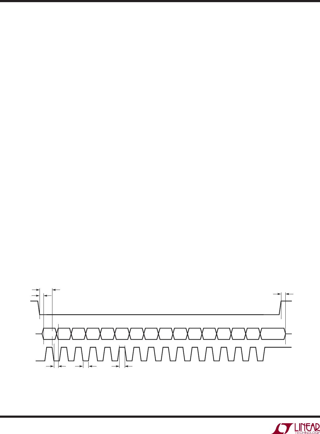
Upon entering the DATA OUTPUT state, SDO outputs the
most signifi cant bit (D15) of the conversion result. During
this state, the ADC shifts the conversion result serially
through the SDO output pin under the control of the SCK
input pin. There is no latency in generating this data and
the result corresponds to the last completed conversion.
A new bit of data appears at the SDO pin following each
falling edge detected at the SCK input pin. The user can
reliably latch this data on every rising edge of the external
serial clock signal driving the SCK pin (see Figure 3).
The DATA OUTPUT state concludes in one of two different
ways. First, the DATA OUTPUT state operation is completed
once all 16 data bits have been shifted out and the clock
then goes low. This corresponds to the 16
th
falling edge
of SCK. Second, the DATA OUTPUT state can be aborted
at any time by a LOW-to-HIGH transition on the CS input.
Following either one of these two actions, the LTC2450-1
will enter the CONVERT state and initiate a new conver-
sion cycle.
Power-Up Sequence
When the power supply voltage V
CC
applied to the con-
verter is below approximately 2.1V, the ADC performs a
power-on reset. This feature guarantees the integrity of
the conversion result.
When V
CC
rises above this critical threshold, the converter
generates an internal power-on reset (POR) signal for
approximately 0.5ms. The POR signal clears all internal
registers. Following the POR signal, the LTC2450-1 starts
a conversion cycle and follows the succession of states
described in Figure 2. The fi rst conversion result fol-
lowing POR is accurate within the specifi cations of the
device if the power supply voltage V
CC
is restored within
the operating range (2.7V to 5.5V) before the end of the
POR time interval.
DATA OUTPUT
SLEEP
CONVERT
POWER-ON RESET
YES
24501 F02
16TH FALLING
EDGE OF SCK
OR
CS = HIGH?
SCK = LOW
AND
CS = LOW?
NO YES
NO
LTC2450-1
8
24501fc
APPLICATIONS INFORMATION
Input Voltage Range
The ADC is capable of digitizing true rail-to-rail input sig-
nals. Ignoring offset and full-scale errors, the converter
will theoretically output an “all zero” digital result when
the input is at ground (a zero scale input) and an “all
one” digital result when the input is at V
CC
(a full-scale
input). In an under-range condition, for all input voltages
less than the voltage corresponding to output code 0, the
converter will generate the output code 0. In an over-range
condition, for all input voltages greater than the voltage
corresponding to output code 65535 the converter will
generate the output code 65535.
Output Data Format
The LTC2450-1 generates a 16-bit direct binary encoded
result. It is provided, MSB fi rst, as a 16-bit serial stream
through the SDO output pin under the control of the SCK
input pin (see Figure 3).
During the data output operation the CS input pin must
be pulled low (CS = LOW). The data output process starts
with the most signifi cant bit of the result being present
at the SDO output pin (SDO = D15) once CS goes low.
A new data bit appears at the SDO output pin following
every falling edge detected at the SCK input pin. The
output data can be reliably latched by the user using the
rising edge of SCK.
Ease of Use
The LTC2450-1 data output has no latency, fi lter settling
delay or redundant results associated with the conversion
cycle. There is a one-to-one correspondence between the
conversion and the output data. Therefore, multiplexing
multiple analog input voltages requires no special ac-
tions.
The LTC2450-1 includes a proprietary input sampling
scheme that reduces the average input current several
orders of magnitude as compared to traditional delta
sigma architectures. This allows external fi lter networks
to interface directly to the LTC2450-1. Since the average
input sampling current is 50nA, an external RC lowpass
lter using a 1kΩ and 0.1μF results in <1LSB error.
Reference Voltage Range
The converter uses the power supply voltage (V
CC
) as the
positive reference voltage (see Figure 1). Thus, the refer-
ence range is the same as the power supply range, which
extends from 2.7V to 5.5V. The LTC2450-1’s internal noise
level is extremely low so the output peak-to-peak noise
remains well below 1LSB for any reference voltage within
this range. Thus the converter resolution remains at 1LSB
independent of the reference voltage. INL, offset, and full-
scale errors vary with the reference voltage as indicated
by the Typical Performance Characteristics graphs. These
error terms will decrease with an increase in the reference
voltage (as the LSB size in μV increases).
Figure 3. Data Output Timing
D
15
LSB
SDO
SCK
D
14
D
13
D
12
D
11
D
10
D
9
D
8
D
7
D
6
D
5
D
4
D
3
D
2
D
0
D
1
24501 F03
t
1
t
3
t
KQ
t
lSCK
t
hSCK
t
2
CS
MSB
LTC2450-1
9
24501fc
Conversion Status Monitor
For certain applications, the user may wish to monitor
the LTC2450-1 conversion status. This can be achieved
by holding SCK HIGH during the conversion cycle. In
this condition, whenever the CS input pin is pulled low
(CS = LOW), the SDO output pin will provide an indication
of the conversion status. SDO = HIGH is an indication of
a conversion cycle in progress while SDO = LOW is an
indication of a completed conversion cycle. An example
of such a sequence is shown in Figure 4.
Conversion status monitoring, while possible, is not required
for LTC2450-1 as its conversion time is fi xed and equal at
approximately 16.6ms (21ms maximum). Therefore, ex-
ternal timing can be used to determine the completion of a
conversion cycle.
SERIAL INTERFACE
The LTC2450-1 transmits the conversion result and receives
the start of conversion command through a synchronous
3-wire interface. This interface can be used during the
CONVERT and SLEEP states to assess the conversion
status and during the DATA OUTPUT state to read the
conversion result, and to trigger a new conversion.
APPLICATIONS INFORMATION
Serial Interface Operation Modes
The following are a few of the more common interface
operation examples. Many more valid control and serial
data output operation sequences can be constructed based
upon the above description of the function of the three
digital interface pins.
The modes of operation can be summarized as follows:
1) The LTC2450-1 functions with SCK idle high (commonly
known as CPOL = 1) or idle low (commonly known as
CPOL = 0).
2) After the 16th bit is read, the user can choose one of
two ways to begin a new conversion. First, one can
pull CS high (CS = ). Second, one can use a high-low
transition on SCK (SCK = ↓).
3) At any time during the Data Output state, pulling CS
high (CS = ) causes the part to leave the I/O state,
abort the output and begin a new conversion.
4) When SCK = HIGH, it is possible to monitor the conver-
sion status by pulling
CS low and watching for SDO
to go low. This feature is available only in the idle-high
(CPOL = 1) mode.
Figure 4. Conversion Status Monitoring Mode
SLEEP
t
1
t
2
SDO
SCK = HI
CONVERT
24501 F04
CS

LTC2450CDC-1#TRPBF

Mfr. #:
Manufacturer:
Analog Devices Inc.
Description:
Analog to Digital Converters - ADC 16-bit 60Hz Delta Sigma ADC in 2x2 DFN
Lifecycle:
New from this manufacturer.
Delivery:
DHL FedEx Ups TNT EMS
Payment:
T/T Paypal Visa MoneyGram Western Union