LTC2450-1
16
24501fc
APPLICATIONS INFORMATION
Figure 16. Measured INL vs Input Voltage,
C
IN
= 0.1μF, V
CC
= 5V, T
A
= 25°C
For most applications, it is desirable to implement C
IN
as
a high quality 0.1μF ceramic capacitor and R
S
≤ 1k. This
capacitor should be located as close as possible to the
actual V
IN
package pin. Furthermore the area encompassed
by this circuit path as well as the path length should be
minimized.
In the case of a 2-wire sensor which is not remotely
grounded, it is desirable to split R
S
and place series
resistors in the ADC input line as well as in the sensor
ground return line which should be tied to the ADC GND
pin using a star connection topology.
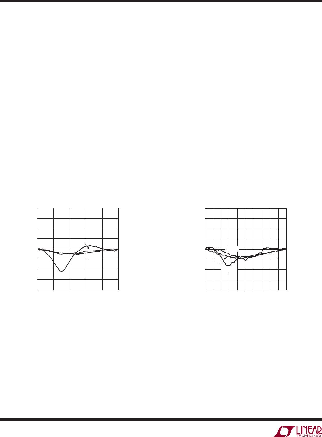
Figure 16 shows the measured LTC2450-1 INL vs
Input Voltage as a function of R
S
value with an input
capacitor C
IN
= 0.1μF.
In some cases, R
S
can be increased above these guide-
lines. The input current is zero while the ADC is either in
sleep or I/O modes. Thus, if the time constant of the input
R-C circuit τ = R
S
• C
IN
is of the same order magnitude or
longer than the time periods between actual conversions,
then one can consider the input current to be reduced
correspondingly.
These considerations need to be balanced out by the input
signal bandwidth. The 3dB bandwidth 1/(2π R
S
C
IN
).
Finally, if the recommended choice for C
IN
is unacceptable
for the users specifi c application, an alternate strategy is to
eliminate C
IN
and minimize C
PAR
and R
S
. In practical terms,
this confi guration corresponds to a low impedance sensor
directly connected to the ADC through minimum length
traces. Actual applications include current measurements
through low value sense resistors, temperature measure-
ments, low impedance voltage source monitoring and so
on. The resultant INL vs V
IN
is shown in Figure 17. The
measurements of Figure 17 include a C
PAR
capacitor cor-
responding to a minimum size layout pad and a minimum
width input trace of about 1 inch length.
Figure 17. Measured INL vs V
IN
, C
IN
= 0, V
CC
= 5V, T
A
= 25°C
INPUT VOLTAGE (V)
0
INL(LSB)
–4
0
4
3
5
24501 F16
–8
–12
–16
12 4
8
12
16
R
S
= 10k
R
S
= 1k
R
S
= 0
INPUT VOLTAGE (V)
0
INL (LSB)
8
6
4
2
0
–2
–4
–6
–8
4
24501 F17
123 53.50.5 1.5 2.5 4.5
R
S
= 1k
R
S
= 10k
R
S
= 0
LTC2450-1
17
24501fc
APPLICATIONS INFORMATION
noise contribution of the external drive circuit would be
V
n
= n
i
• √π/2 • F
i
. Then, the total system noise level can
be estimated as the square root of the sum of (V
n
2
) and
the square of the LTC2450-1 noise fl oor (≈2μV
2
).
Aliasing
The LTC2450-1 signal acquisition circuit is a sampled
data system and as such suffers from input signal alias-
ing. As can be seen from Figure 19, due to the very high
over-sample ratios the high frequency input signal attenu-
ation is reasonably good. Nevertheless a continuous time
antialiasing fi lter connected at the input will preserve
the converter accuracy when the input signal includes
undesirable high frequency components. The antialias-
ing function can be accomplished using the R
S
and C
IN
components shown in Figure 15 sized such that τ = R
S
• C
IN
> 450ns.
Figure 18. Input Signal Attenuation vs Frequency
(Low Frequencies)
Figure 19. Input Signal Attenuation vs Frequency
Signal Bandwidth and Noise Equivalent Input
Bandwidth
The LTC2450-1 includes a sinc
1
type digital fi lter with the
rst notch located at f
0
= 60Hz. As such the 3dB input
signal bandwidth is 26.54Hz. The calculated LTC2450-1
input signal attenuation with frequency at low frequencies
is shown in Figure 18.
The LTC2450-1 input signal attenuation with frequency
over a wide frequency range is shown in Figure 19.
The converter noise level is about 1.4μV
RMS
and can be
modeled by a white noise source connected at the input
of a noise free converter.
For a simple system noise analysis the V
IN
drive circuit can
be modeled as a single pole equivalent circuit character-
ized by a pole location F
i
and a noise spectral density n
i
.
If the converter has an unlimited bandwidth or at least
a bandwidth substantially larger than F
i
, then the total
INPUT SIGNAL FREQUENCY (Hz)
0
INPUT SIGNAL ATTENUATIOIN (dB)
–20
–10
0
480
24501 F18
–30
–40
–25
–15
–5
–35
–45
–50
12060
240180
360 420 540
300
600
INPUT SIGNAL FREQUENCY (MHz)
0
INPUT SIGNAL ATTENUATION (dB)
–40
0
10.0 12.5 15.0
24501 F19
–60
–80
–20
–100
2.5
5.0 7.5
LTC2450-1
18
24501fc
Thermistor Measurement
TYPICAL APPLICATION
CS
V
CC
LTC2450-1
5V
GND
SCK
V
IN
100nF
10k
THERMISTOR
1k TO 10k
SDO
24501 TA02

LTC2450CDC-1#TRPBF

Mfr. #:
Manufacturer:
Analog Devices Inc.
Description:
Analog to Digital Converters - ADC 16-bit 60Hz Delta Sigma ADC in 2x2 DFN
Lifecycle:
New from this manufacturer.
Delivery:
DHL FedEx Ups TNT EMS
Payment:
T/T Paypal Visa MoneyGram Western Union