AT17LV65A/128A/256A/512A/002A [DATASHEET]
Atmel-2322I-FPGA-AT17LV65A-128A-256A-512A-002A-Datasheet_102014
2
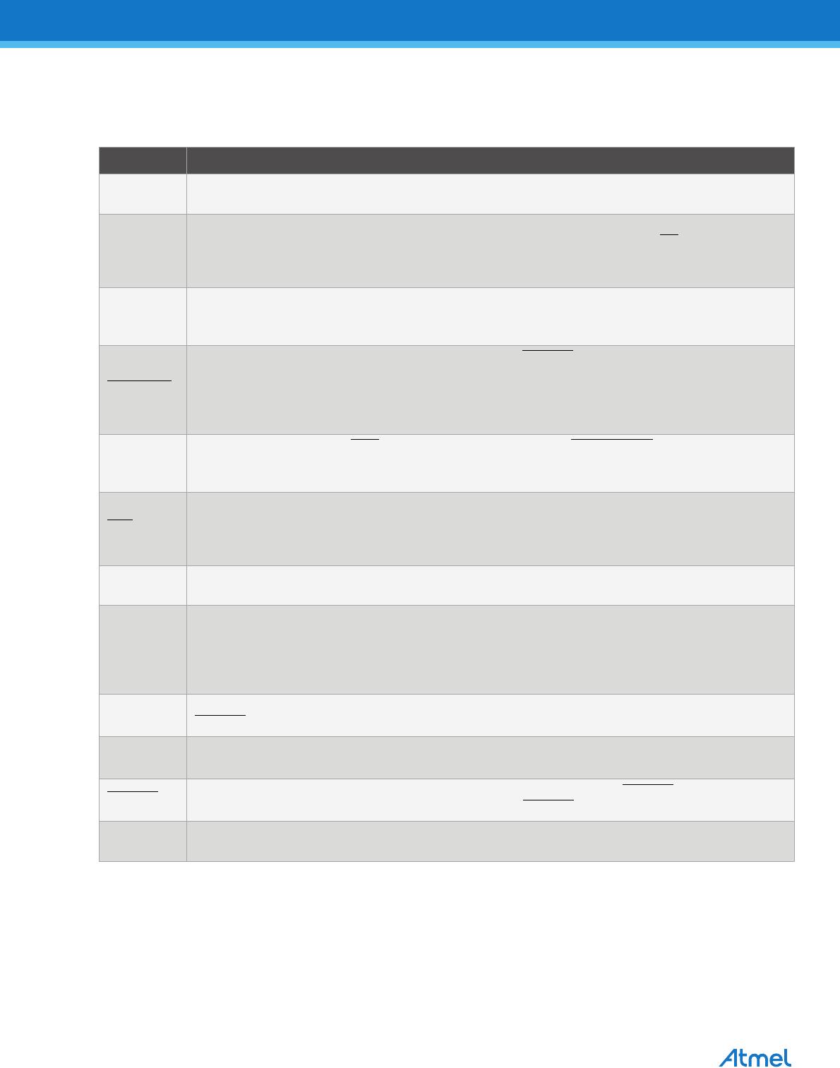
1. Pin Configuration and Descriptions
Table 1-1. Pin Descriptions
Pin Description
DATA Three-state DATA Output for Configuration. Open-collector bi-directional pin for programming.
DCLK
Clock Output or Clock Input. Rising edges on DCLK increment the internal address counter and present
the next bit of data to the DATA pin. The counter is incremented only if the RESET/
OE input is held High,
the nCS input is held Low, and all configuration data has not been transferred to the target device
(otherwise, as the master device, the DCLK pin drives Low).
WP1
Write Protect (1). This pin is used to protect portions of memory during programming, and it is disabled
by default due to internal pull-down resistor. This input pin is not used during FPGA loading operations.
This pin is only available on the AT17LV512A/010A/002A.
RESET/OE
RESET (Active Low) / Output Enable (Active High) when SER_EN is High. A Low logic level resets the
address counter. A High logic level (with nCS Low) enables DATA and permits the address counter to
count. In the mode, if this pin is Low (reset), the internal oscillator becomes inactive and DCLK drives Low.
The logic polarity of this input is programmable and must be programmed active High (RESET active Low)
by the user during programming for Altera applications.
WP
Write Protect Input (when nCS is Low) during programming only (SER_EN Low). When WP is Low, the
entire memory can be written. When WP is enabled (High), the lowest block of the memory cannot be
written. This pin is only available on AT17LV65A/128A/256A devices.
nCS
Chip Select Input (Active Low). A Low input (with OE High) allows DCLK to increment the address
counter and enables DATA to drive out. If the AT17LVxxxA is reset with nCS Low, the device initializes as
the first (and master) device in a daisy-chain. If the AT17LVxxxA is reset with nCS High, the device
initializes as a subsequent AT17LVxxxA in the chain.
GND Ground. A 0.2μF decoupling capacitor between V
CC
and GND is recommended.
nCASC
Cascade Select Output (Active Low). This output goes Low when the address counter has reached its
maximum value. In a daisy-chain of AT17LVxxxA devices, the nCASC pin of one device is usually
connected to the nCS input pin of the next device in the chain, which permits DCLK from the master
configurator to clock data from a subsequent AT17LVxxxA device in the chain. This feature is not available
on the AT17LV65A (NRND).
A2
Device Selection Input, A2. This is used to enable (or select) the device during programming (i.e., when
SER_EN is Low). A2 has an internal pull-down resistor.
READY
Open Collector Reset State Indicator. Driven Low during power-on reset cycle, released when power-
up is complete. (recommended 4.7k pull-up on this pin if used).
SER_EN
Serial Enable must be held High during FPGA loading operations. Bringing SER_EN Low enables the 2-
wire Serial Programming Mode. For non-ISP applications,
SER_EN should be tied to V
CC
.
V
CC
Power Supply. 3.3V (±10%) and 5.0V (±10%) power supply pin.