AT17LV65A/128A/256A/512A/002A [DATASHEET]
Atmel-2322I-FPGA-AT17LV65A-128A-256A-512A-002A-Datasheet_102014
4
2. Block Diagram
Figure 2-1. Block Diagram
Notes: 1. This pin is only available on AT17LV65A/128A/256A (NRND).
2. This pin is only available on AT17LV512A/010A/002A.
3. The nCASC feature is not available on the AT17LV65A (NRND).
Power On
Reset
SER_EN
WP1
(2)
READY
(2)
DCLK
nCS
nCASC
RESET/OE
(WP
(1)
)
Oscillator
Oscillator
Controll
Programming
Mode Logic
Programming
Data Shift
Register
EEPROM
Cell
Matrix
Row
Decoder
Row
Address
Counter
Bit
Counter
Column
Decoder
5
AT17LV65A/128A/256A/512A/002A [DATASHEET]
Atmel-2322I-FPGA-AT17LV65A-128A-256A-512A-002A-Datasheet_102014
3. Device Description
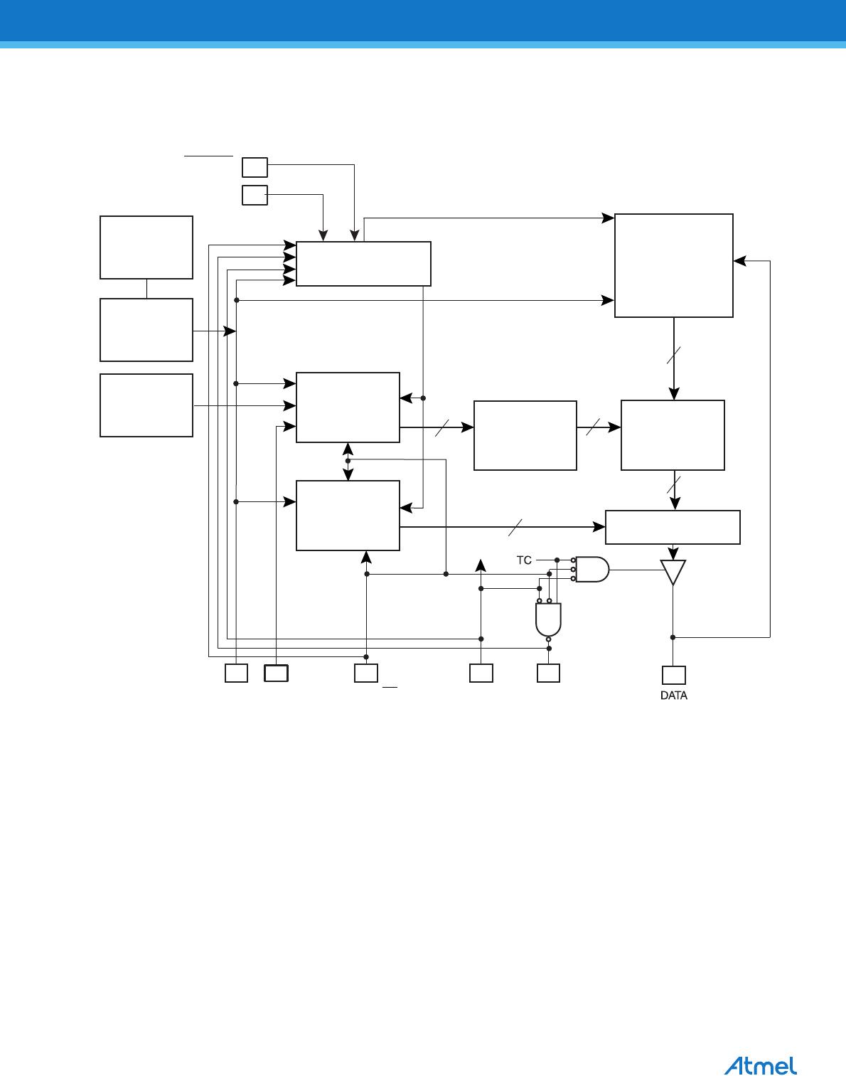
The control signals for the configuration EEPROM (nCS, RESET/OE and DCLK) interface directly with the
FPGA device control signals. All FPGA devices can control the entire configuration process and retrieve data
from the configuration EEPROM without requiring an external controller.
The configuration EEPROM’s RESET/OE and nCS pins control the tri-state buffer on the DATA output pin and
enable the address counter and the oscillator. When RESET/OE is driven Low, the configuration EEPROM
resets its address counter and tri-states its DATA pin. The nCS pin also controls the output of the AT17LVxxxA
configurator. If nCS is held High after the RESET/OE pulse, the counter is disabled and the DATA output pin is
tri-stated. When nCS is driven subsequently Low, the counter and the DATA output pin are enabled. When
RESET/OE is driven Low again, the address counter is reset and the DATA output pin is tri-stated, regardless of
the state of the nCS.
When the configurator has driven out all of its data and nCASC is driven Low, the device tri-states the DATA pin
to avoid contention with other configurators. Upon power-up, the address counter is automatically reset.
This is the default setting for the device. Since almost all FPGAs use RESET Low and OE High, this document
will describe RESET/OE.
4. FPGA Master Serial Mode Summary
The I/O and logic functions of any SRAM-based FPGA are established by a configuration program. The
program is loaded either automatically upon power-up, or on command, depending on the state of the FPGA
mode pins. In Master mode, the FPGA automatically loads the configuration program from an external memory.
The AT17LVxxxA Serial Configuration EEPROM has been designed for compatibility with the Master Serial
mode.
This document discusses the Altera FLEX FPGA device interfaces.
5. Control of Configuration
Most connections between the FPGA device and the AT17LVxxxA Serial EEPROM are simple and self-
explanatory.
The DATA output of the AT17LVxxxA configurator drives DIN of the FPGA devices.
The master FPGA DCLK output or external clock source drives the DCLK input of the AT17LVxxxA
configurator.
The nCASC output of any AT17LVxxxA configurator drives the nCS input of the next configurator in a
cascaded chain of EEPROMs.
SER_EN must be connected to V
CC
(except during ISP).
AT17LV65A/128A/256A/512A/002A [DATASHEET]
Atmel-2322I-FPGA-AT17LV65A-128A-256A-512A-002A-Datasheet_102014
6
6. Cascading Serial Configuration EEPROMs
For multiple FPGAs configured as a daisy-chain, or for FPGAs requiring larger configuration memories,
cascaded configurators provide additional memory.
After the last bit from the first configurator is read, the next clock signal to the configurator asserts its nCASC
output low and disables its DATA line driver. The second configurator recognizes the low level on its nCS input
and enables its DATA output.
After configuration is complete, the address counters of all cascaded configurators are reset if the RESET/OE
on each configurator is driven to a Low level.
If the address counters are not to be reset upon completion, then the RESET/OE input can be tied to a High
level.
The AT17LV65A (NRND) does not have the nCASC feature to perform cascaded configurations.
7. AT17LVxxxA Reset Polarity
The AT17LVxxxA configurator allows the user to program the polarity of the RESET/OE pin as either
RESET/OE or RESET/OE. This feature is supported by industry-standard programmer algorithms.
8. Programming Mode
The programming mode is entered by bringing SER_EN Low. In this mode the chip can be programmed by the
2-wire serial bus. The programming is done at V
CC
supply only. Programming super voltages are generated
inside the chip.
9. Standby Mode
The AT17LVxxxA enters a low-power standby mode whenever nCS is asserted High. In this mode,
the configurator consumes less than 150μA of current at 3.3V. The output remains in a high-impedance state
regardless of the state of the RESET/OE input.

AT17LV002A-10JU

Mfr. #:
Manufacturer:
Microchip Technology / Atmel
Description:
FPGA - Configuration Memory CONFIG SER EEPROM-2M ALTERA PINOUT-10MHZ
Lifecycle:
New from this manufacturer.
Delivery:
DHL FedEx Ups TNT EMS
Payment:
T/T Paypal Visa MoneyGram Western Union