7
AT17LV65A/128A/256A/512A/002A [DATASHEET]
Atmel-2322I-FPGA-AT17LV65A-128A-256A-512A-002A-Datasheet_102014
10. Electrical Specifications
10.1 Absolute Maximum Ratings*
10.2 Operating Conditions
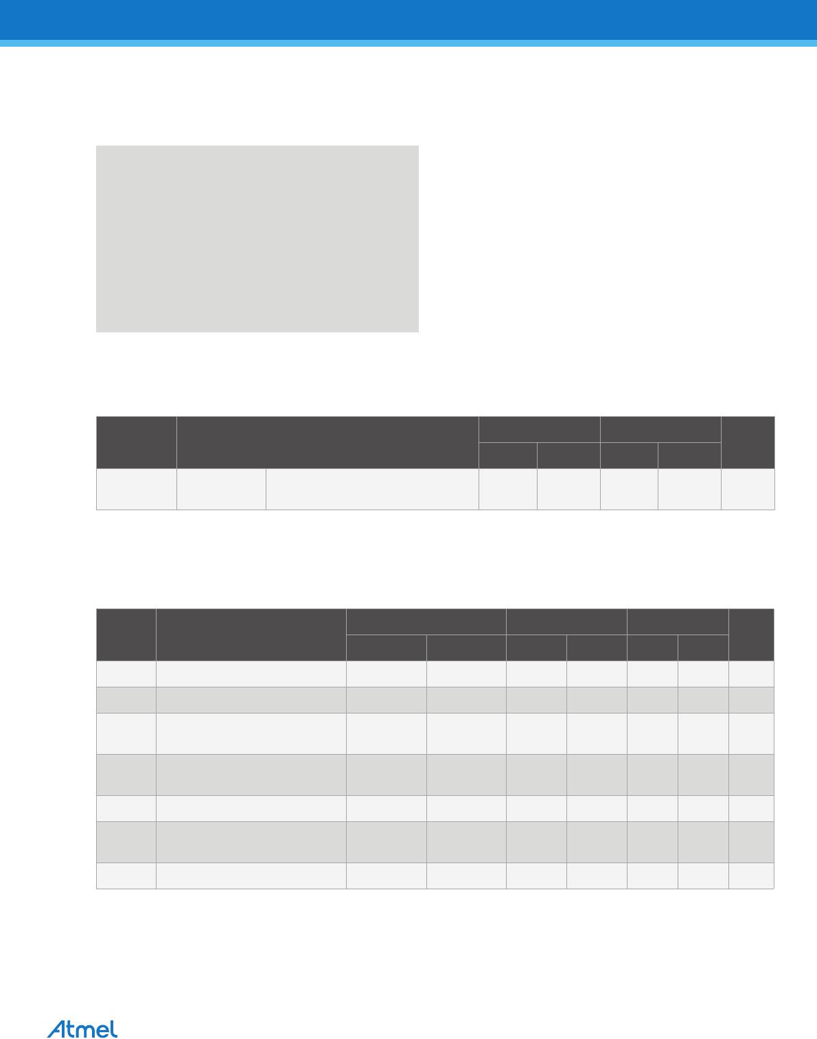
Table 10-1. Operating Conditions
10.3 DC Characteristics
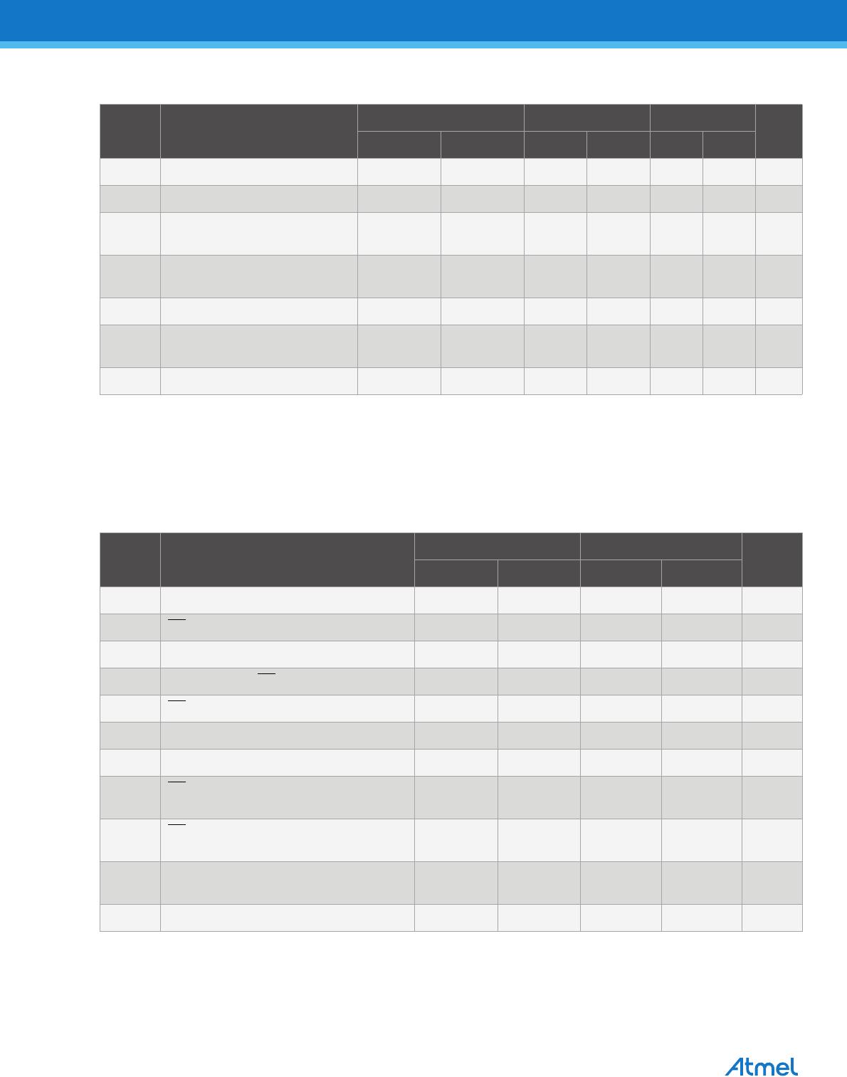
Table 10-2. DC Characteristics for V
CC
= 3.3V ± 10%
Note: 1. The AT17LV65A, AT17LV128A, and AT17LV256A are not recommended for new designs.
Operating Temperature . . . . . . . . . . . .-40C to +85C
Storage Temperature . . . . . . . . . . . . .-65C to +150C
Voltage on Any Pin
with Respect to Ground . . . . . . . . . -0.1V to V
CC
+0.5V
Supply Voltage (V
CC
) . . . . . . . . . . . . . . -0.5V to +7.0V
Maximum Soldering Temp. (10s @ 1/16 in.) . . . 260C
ESD (R
ZAP
= 1.5K, C
ZAP
= 100 pF)2000V
*Notice: Stresses beyond those listed under Absolute
Maximum Ratings may cause permanent damage
to the device. This is a stress rating only and
functional operation of the device at these or any
other conditions beyond those listed under
operating conditions is not implied. Exposure to
Absolute Maximum Rating conditions for extended
periods of time may affect device reliability.
Symbol Description
3.3V 5.0V
UnitsMin Max Min Max
V
CC
Industrial
Supply voltage relative to GND
-40C to +85C
3.0 3.6 4.5 5.5 V
Symbol Description
AT17LV65A/128A/256A
(1)
AT17LV512A/010A AT17LV002A
UnitsMin Max Min Max Min Max
V
IH
High-level Input Voltage
2.0 V
CC
2.0 V
CC
2.0 V
CC
V
V
IL
Low-level Input Voltage
0 0.8 0 0.8 0 0.8 V
V
OH
High-level Output Voltage
(I
OH
= -2mA)
2.4 2.4 2.4 V
V
OL
Low-level Output Voltage
(I
OL
= +3mA)
0.4 0.4 0.4 V
I
CCA
Supply Current, Active Mode
5 5 5 mA
I
L
Input or Output Leakage Current
(V
IN
= V
CC
or GND)
-10 10 -10 10 -10 10 μA
I
CCS
Supply Current, Standby Mode
100 100 150 μA