X9119
3
FN8162.5
July 5, 2016
Submit Document Feedback
Bus Interface Pins
SERIAL DATA INPUT/OUTPUT (SDA)
The SDA is a bidirectional serial data input/output pin for a
2-wire slave device and is used to transfer data into and out of
the device. It receives device address, opcode, wiper register
address and data sent from a 2-wire master at the rising edge of
the serial clock SCL, and it shifts out data after each falling edge
of the serial clock SCL.
It is an open-drain output and may be wire-ORed with any
number of open-drain or open collector outputs. An open-drain
output requires the use of a pull-up resistor. For selecting typical
values, refer to the guidelines for calculating typical values on the
bus pull-up resistors graph.
SERIAL CLOCK (SCL)
This input is used by a 2-wire master to supply a 2-wire serial
clock to the X9119.
DEVICE ADDRESS (A
2
–A
0
)
The Address inputs are used to set the least significant 3 bits of
the 8-bit slave address. A match in the slave address serial data
stream must be made with the Address input in order to initiate
communication with the X9119. A maximum of 8 devices may
occupy the 2-wire serial bus.
HARDWARE WRITE PROTECT INPUT (WP)
The WP pin when LOW, prevents nonvolatile writes to the Data
Registers.
Potentiometer Pins
R
H
, R
L
The R
H
and R
L
pins are equivalent to the terminal connections on
a mechanical potentiometer.
R
W
The wiper pin are equivalent to the wiper terminal of a
mechanical potentiometer.
Bias Supply Pins
SYSTEM SUPPLY VOLTAGE (V
CC
) AND SUPPLY
GROUND (V
SS
)
The V
CC
pin is the system supply voltage. The V
SS
pin is the
system ground.
Other Pins
NO CONNECT
No connect pins should be left open. These pins are used for
Intersil manufacturing and testing purposes.
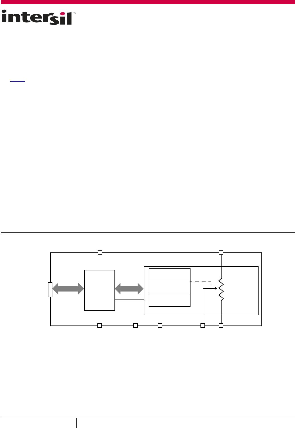
Principals of Operation
The X9119 is an integrated microcircuit incorporating a resistor
array and its associated registers and counters and the serial
interface logic providing direct communication between the host
and the digitally controlled potentiometer. This section provides
detail description of the following:
• Resistor Array Description
• Serial Interface Description
• Instruction and Register Description
Resistor Array Description
The X9119 is comprised of a resistor array. The array contains, in
effect, 1023 discrete resistive segments that are connected in
series (Figure 3 on page 4
). The physical ends of each array are
equivalent to the fixed terminals of a mechanical potentiometer
(R
H
and R
L
inputs).
At both ends of each array and between each resistor segment is
a CMOS switch connected to the wiper (R
W
) output. Within each
individual array only one switch may be turned on at a time.
These switches are controlled by the Wiper Counter Register
(WCR). The 10-bits of the WCR (WCR[9:0]) are decoded to select,
and enable, one of 1024 switches.
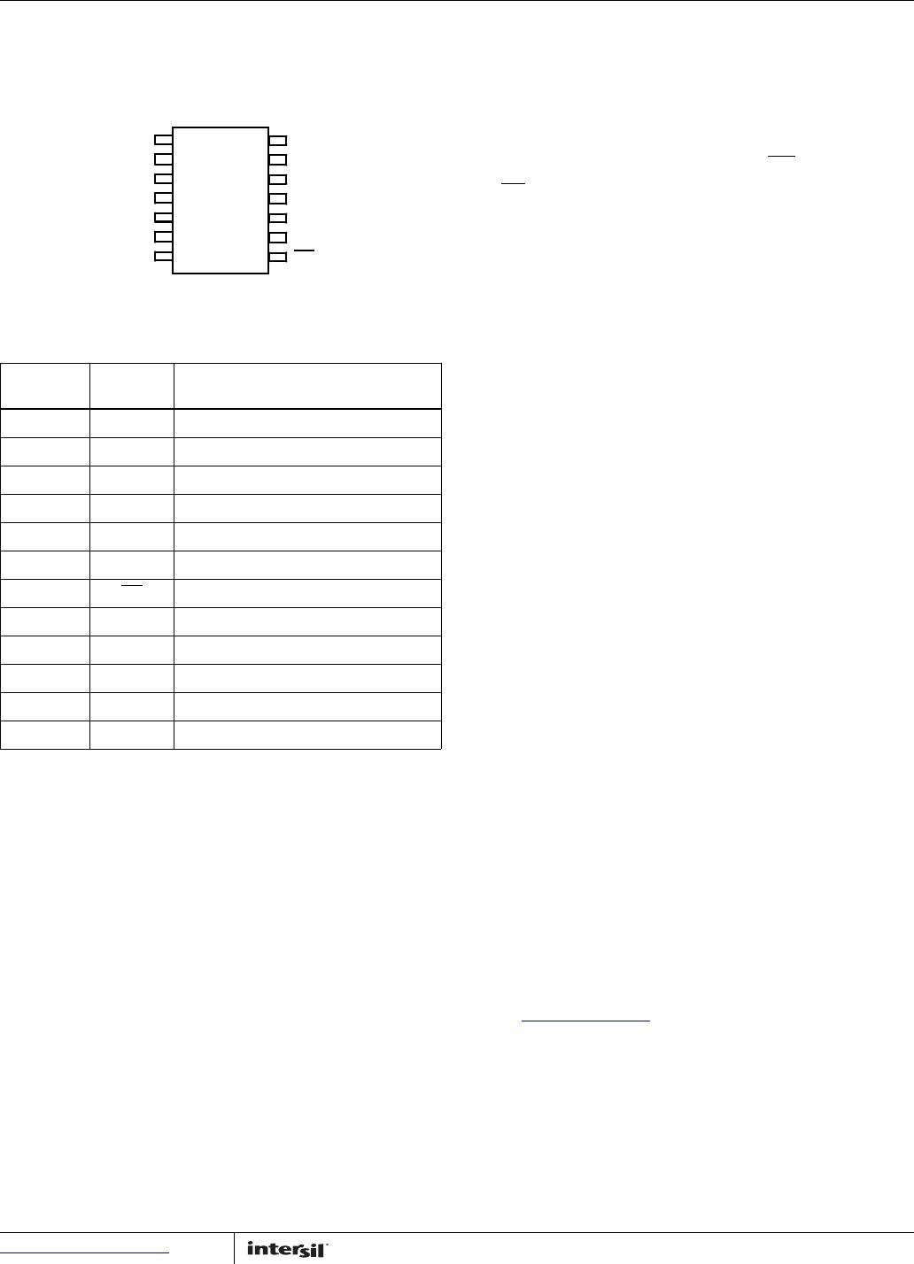
Pin Configuration
X9119
(14 LD TSSOP)
TOP VIEW
Pin Assignments
PIN
NUMBER PIN NAME FUNCTION
1, 3, 10 NC No connect
2 A0 Device address for 2-wire bus
4 A2 Device address for 2-wire bus
5 SCL Serial clock for 2-wire bus
6 SDA Serial data input/output for 2-wire bus
7V
SS
System ground
8WP
Hardware write protect
9 A1 Device address for 2-wire bus
11 R
W
Wiper terminal of the potentiometer
12 R
H
High terminal of the potentiometer
13 R
L
Low terminal of the potentiometer
14 V
CC
System supply voltage
V
CC
R
L
V
SS
1
2
3
4
5
6
7
8
14
13
12
11
10
9
NC
R
W
A2
A1
R
H
A0
NC
SDA
NC
SCL
WP