X9119
4
FN8162.5
July 5, 2016
Submit Document Feedback
The WCR may be written directly. The data registers and the WCR
can be read and written by the host system.
Serial Interface Description
SERIAL INTERFACE
The X9119 supports a bidirectional bus oriented protocol. The
protocol defines any device that sends data onto the bus as a
transmitter and the receiving device as the receiver. The device
controlling the transfer is a master and the device being
controlled is the slave. The master will always initiate data
transfers and provide the clock for both transmit and receive
operations. Therefore, the X9119 will be considered a slave
device in all applications.
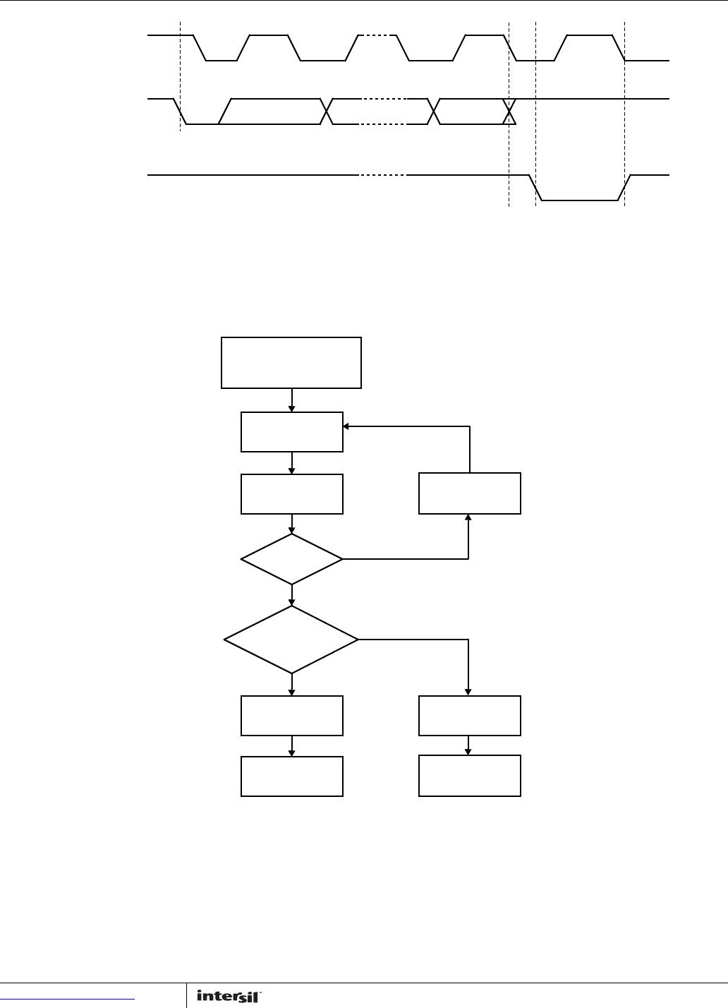
CLOCK AND DATA CONVENTIONS
Data states on the SDA line can change only during SCL LOW
periods. SDA state changes during SCL HIGH are reserved for
indicating start and stop conditions (Figure 6 on page 8).
START CONDITION
All commands to the X9119 are preceded by the start condition,
which is a HIGH to LOW transition of SDA while SCL is HIGH. The
X9119 continuously monitors the SDA and SCL lines for the start
condition and will not respond to any command until this
condition is met (Figure 6
).
STOP CONDITION
All communications must be terminated by a stop condition,
which is a LOW to HIGH transition of SDA while SCL is HIGH (see
Figure 6
).
ACKNOWLEDGE
Acknowledge is a software convention used to provide a positive
handshake between the master and slave devices on the bus to
indicate the successful receipt of data. The transmitting device,
either the master or the slave, will release the SDA bus after
transmitting eight bits. The master generates a ninth clock cycle
and during this period the receiver pulls the SDA line LOW to
acknowledge that it successfully received the eight bits of data.
The X9119 will respond with an acknowledge after recognition of
a start condition and its slave address and once again after
successful receipt of the command byte. If the command is
followed by a data byte the X9119 will respond with a final
acknowledge (see Figure 4
).
ACKNOWLEDGE POLLING
The disabling of the inputs, during the internal nonvolatile write
operation, can be used to take advantage of the typical 5ms
EEPROM write cycle time. Once the stop condition is issued to
indicate the end of the nonvolatile write command the X9119
initiates the internal write cycle. ACK polling, Flow 1 (see
Figure 5 on page 5
), can be initiated immediately. This involves
issuing the start condition followed by the device slave address. If
the X9119 is still busy with the write operation, no ACK will be
returned. If the X9119 has completed the write operation, an
ACK will be returned and the master can then proceed with the
next operation.
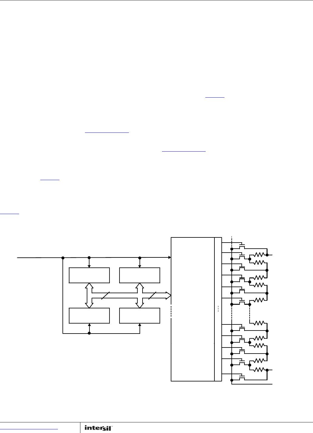
FIGURE 3. DETAILED POTENTIOMETER BLOCK DIAGRAM SERIAL INTERFACE DESCRIPTION
SERIAL DATA PATH
FROM INTERFACE
REGISTER 0
SERIAL
BUS
INPUT
PARALLEL
BUS
INPUT
COUNTER
REGISTER
R
H
R
L
R
W
10 10
C
O
U
N
T
E
R
D
E
C
O
D
E
WIPER
(WCR)
(DR0)
CIRCUITRY
REGISTER 1
(DR1)
REGISTER 2
(DR2)
REGISTER 3
(DR3)
R
IF WCR = 000[HEX] THEN R
W
= R
L
IF WCR = 3FF[HEX] THEN R
W
= R
H
X9119
5
FN8162.5
July 5, 2016
Submit Document Feedback
FIGURE 4. ACKNOWLEDGE RESPONSE FROM RECEIVER
FIGURE 5. FLOW 1. ACK POLLING SEQUENCE
SCL FROM
MASTER
DATA OUTPUT
FROM TRANSMITTER
1
89
ST AR T
ACKNOWLEDGE
DATA OUTPUT
FROM RECEIVER
NONVOLATILE WRITE
COMMAND COMPLETED
ENTER ACK POLLING
ISSUE
START
ISSUE SLAVE
ADDRESS
ACK
RETURNED?
FURTHER
OPERATION?
ISSUE
INSTRUCTION
ISSUE STOP
NO
YES
YES
PROCEED
ISSUE STOP
NO
PROCEED
X9119
6
FN8162.5
July 5, 2016
Submit Document Feedback
Instruction and Register
Description
Device Addressing: Identification Byte
(ID and A)
Following a start condition, the master must output the address
of the slave it is accessing. The most significant four bits of the
slave address are the device type identifier. The ID[3:0] bits is the
device ID for the X9119; this is fixed as 0101[B] (refer to Table 1
).
The A2–A0 bits in the ID byte is the internal slave address. The
physical device address is defined by the state of the A2–A0
input pins. The slave address is externally specified by the user.
The X9119 compares the serial data stream with the address
input state; a successful compare of both address bits is required
for the X9119 to successfully continue the command sequence.
Only the device which slave address matches the incoming
device address sent by the master executes the instruction. The
A2–A0 inputs can be actively driven by CMOS input signals or
tied to V
CC
or V
SS
. The R/W bit is the LSB and is be used to
program the device for read or write operations.
INSTRUCTION BYTE AND REGISTER SELECTION
The next byte sent to the X9119 contains the instruction and
register pointer information. The three most significant bits are
used provide the instruction opcode (IOP[2:0]). The RB and RA
bits point to one of the four registers. The format is shown in
Table 2
.
Table 3
provides a complete summary of the instruction set
opcodes.
TABLE 1. IDENTIFICATION BYTE FORMAT
TABLE 2. INSTRUCTION BYTE FORMAT
ID3 ID2 ID1 ID0 A2 A1 A0 R/W
0101
(MSB) (LSB)
DEVICE TYPE
IDENTIFIES
INTERNAL SLAVE
ADDRESS
READ OR
WRITE BIT
I2 I1 I0 0 RB RA 0 0
(MSB) (LSB)
INSTRUCTION
OPCODE
REGISTER
SELECTION
REGISTER SELECTED RB RA
DR0 0 0
DR1 0 1
DR2 1 0
DR3 1 1
TABLE 3. INSTRUCTION SET
INSTRUCTION
INSTRUCTION SET
OPERATIONR/W
I
2
I
1
I
0
0RBRA 0 0
Read Wiper Counter Register 1 1 0 0 0 0 0 0 0 Read the contents of the wiper counter register.
Write Wiper Counter Register 0 1 0 1 0 0 0 0 0 Write new value to the wiper counter register.
Read Data Register 1 1 0 1 0 1/0 1/0 0 0 Read the contents of the data register pointed to
RB-RA.
Write Data Register 0 1 1 0 0 1/0 1/0 0 0 Write new value to the data register pointed to RB-RA.
XFR Data Register to Wiper
Counter Register
1 1 1 0 0 1/0 1/0 0 0 Transfer the contents of the data register pointed to by
RB-RA to the wiper counter register.
XFR Wiper Counter Register to
Data Register
0 1 1 1 0 1/0 1/0 0 0 Transfer the contents of the wiper counter register to
the data register pointed to by RB-RA.
NOTE: 1/0 = data is one or zero.

X9119TV14Z-2.7

Mfr. #:
Manufacturer:
Renesas / Intersil
Description:
Digital Potentiometer ICs SINGLE DCP 100KOHM 1024 TAP 2-WIRE COM
Lifecycle:
New from this manufacturer.
Delivery:
DHL FedEx Ups TNT EMS
Payment:
T/T Paypal Visa MoneyGram Western Union