X9119
10
FN8162.5
July 5, 2016
Submit Document Feedback
Absolute Maximum Ratings
Voltage on SCL, SDA, or any address input
with respect to V
SS
. . . . . . . . . . . . . . . . . . . . . . . . . . . . . . . . . . . . . .-1V to +7V
V = | (VH–VL) | . . . . . . . . . . . . . . . . . . . . . . . . . . . . . . . . . . . . . . . . . . . . . . 5V
I
W
(10s) . . . . . . . . . . . . . . . . . . . . . . . . . . . . . . . . . . . . . . . . . . . . . . . . . . ±6mA
Operating Conditions
Commercial. . . . . . . . . . . . . . . . . . . . . . . . . . . . . . . . . . . . . . . . 0°C to +70°C
Industrial . . . . . . . . . . . . . . . . . . . . . . . . . . . . . . . . . . . . . . . . . -40° to +85°C
Supply Voltage (V
CC
) Limits (Note 9)
X9119 . . . . . . . . . . . . . . . . . . . . . . . . . . . . . . . . . . . . . . . . . . . . . . .5V ±10%
X9119-2.7 . . . . . . . . . . . . . . . . . . . . . . . . . . . . . . . . . . . . . . . . . 2.7V to 5.5V
Thermal Information
Temperature under bias . . . . . . . . . . . . . . . . . . . . . . . . . . .-65°C to +135°C
Storage temperature . . . . . . . . . . . . . . . . . . . . . . . . . . . . . .-65°C to +150°C
Lead temperature (soldering, 10s). . . . . . . . . . . . . . . . . . . . . . . . . . . . 300°C
Pb-Free Reflow Profile . . . . . . . . . . . . . . . . . . . . . . . . . . . . . . . . . . see TB493
CAUTION: Do not operate at or near the maximum ratings listed for extended periods of time. Exposure to such conditions may adversely impact product
reliability and result in failures not covered by warranty.
Analog Specifications (Over recommended operation conditions unless otherwise stated.)
PARAMETER SYMBOL TEST CONDITIONS
MIN
(Note 13
)TYP
MAX
(Note 13)UNIT
End-to-End Resistance R
TOTAL
100 kΩ
End-to-End Resistance Tolerance ±20 %
Power Rating +25°C, each pot 50 mW
Wiper Current I
W
±3 mA
Wiper Resistance R
W
Wiper Current = ± 50µA,
V
CC
= 5V
40 110 Ω
Wiper Current = ± 50µA,
V
CC
= 3V
150 300 Ω
Voltage on any R
H
or R
L
Pin V
TERM
V
SS
= 0V V
SS
5V
Noise Ref: 1V -120 dBV
Resolution 0.1 %
Absolute Linearity (Note 6
)R
w(n)(actual)
– R
w(n)(expected)
, where n = 8 to
1006
±1.5 MI
(Note 8
)
R
w(n)(actual)
– R
w(n)(expected)
(Note 91.5±2.0MI
(Note 8
)
Relative Linearity (Note 7
)R
w(m + 1)
– [R
w(m)
+ MI], where m = 8 to
1006
±0.5 MI
(Note 8
)
R
w(m + 1)
– [R
w(m)
+ MI] (Note 9) ±0.5 ±1.0 MI
(Note 8
)
Temperature Coefficient of R
TOTAL
±300 ppm/°C
Ratiometric Temperature Coefficient 20 ppm/°C
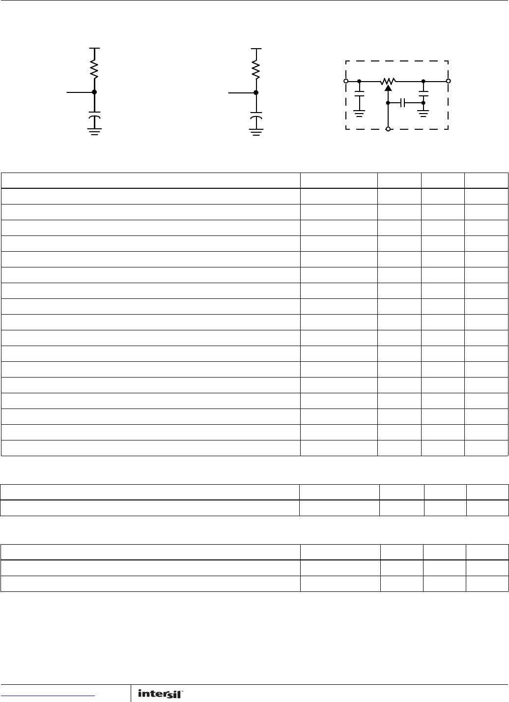
Potentiometer Capacitances C
H
/C
L
/C
W
See Macro model 10/10/25 pF
NOTES:
6. Absolute linearity is utilized to determine actual wiper voltage vs expected voltage as determined by wiper position when used as a potentiometer.
7. Relative linearity is utilized to determine the actual change in voltage between two successive tap positions when used as a
potentiometer. It is a measure of the error in step size.
8. MI = R
TOT
/1023 or (R
H
– R
L
)/1023, single potentiometer
9. n = 0, 1, 2, …,1023; m = 0, 1, 2, …, 1022.
10. ESD Rating on R
H
, R
L
, R
W
pins is 1.5kV (HBM, 1.0µA leakage maximum), ESD rating on all other pins is 2.0kV.
X9119
11
FN8162.5
July 5, 2016
Submit Document Feedback
Operating Specifications (Over the recommended operating conditions unless otherwise specified.)
PARAMETER SYMBOL TEST CONDITIONS MIN TYP MAX UNIT
V
CC
Supply Current (Active) I
CC1
f
SCL
= 400kHz; V
CC
= +5.5V;
SDA = Open; (for 2-wire, active, read and volatile write states only)
3mA
V
CC
Supply Current
(Nonvolatile Write)
I
CC2
f
SCL
= 400kHz; V
CC
= +5.5V;
SDA = Open; (for 2-wire, active, non-volatile write state only)
5mA
V
CC
Current (Standby) I
SB
V
CC
= +5.5V; V
IN
= V
SS
or V
CC
; SDA = V
CC
;
(for 2-wire, standby state only)
A
Input Leakage Current I
LI
V
IN
= V
SS
to V
CC
10 µA
Output Leakage Current I
LO
V
OUT
= V
SS
to V
CC
10 µA
Input HIGH Voltage V
IH
V
CC
x 0.7 V
CC
+ 1 V
Input LOW Voltage V
IL
-1 V
CC
x 0.3 V
Output LOW Voltage V
OL
I
OL
= 3mA 0.4 V
Output HIGH Voltage V
OH
Endurance and Data Retention
PARAMETER MIN UNITS
Minimum Endurance 100,000 Data changes per bit per register
Data Retention 100 years
Capacitance
TEST SYMBOL TEST CONDITIONS MAX UNIT
Input/Output Capacitance (SI) C
IN/OUT
(Note 11)V
OUT
= 0V 8 pF
Input Capacitance (SCL, WP, A1 and A0) C
IN
(Note 11)V
IN
= 0V 6 pF
Power-Up Timing
PARAMETER SYMBOL MIN MAX UNIT
V
CC
Power-Up Rate t
r
V
CC
(Note 11)0.2 50 V/ms
Power-Up to Initiation Of Read Operation t
PUR
(Note 12)1ms
Power-Up to Initiation Of Write Operation t
PUW
(Note 12)50ms
NOTES:
11. Limits should be considered typical and are not production tested.
12. t
PUR
and t
PUW
are the delays required from the time the (last) power supply (Vcc-) is stable until the specific instruction can be issued. These
parameters are not 100% tested.
13. Parameters with MIN and/or MAX limits are 100% tested at +25°C, unless otherwise specified. Temperature limits established by characterization
and are not production tested.
AC Test Conditions
Input Pulse Levels V
CC
x 0.1 to V
CC
x 0.9
Input Rise and Fall Times 10ns
Input and Output Timing Level V
CC
x 0.5
X9119
12
FN8162.5
July 5, 2016
Submit Document Feedback
Equivalent A.C. Load Circuit
R
H
10pF
C
L
C
L
R
W
R
TOTAL
C
W
25pF
10pF
R
L
SPICE MACROMODEL
5V
1533Ω
100pF
SDA OUTPUT
3V
867Ω
100pF
SDA OUTPUT
AC Timing High-Voltage Write Cycle Timing
PARAMETER SYMBOL MIN MAX UNIT
Clock Frequency f
SCL
400 kHz
Clock Cycle Time t
CYC
2500 ns
Clock High Time t
HIGH
600 ns
Clock Low Time t
LOW
1300 ns
Start Set-Up Time t
SU:STA
600 ns
Start Hold Time t
HD:STA
600 ns
Stop Set-Up Time t
SU:STO
600 ns
SDA Data Input Set-Up Time t
SU:DAT
100 ns
SDA Data Input Hold Time t
HD:DAT
0ns
SCL and SDA Rise Time t
R
300 ns
SCL and SDA Fall Time t
F
300 ns
SCL Low to SDA Data Output Valid Time t
AA
250 ns
SDA Data Output Hold Time t
DH
0ns
Noise Suppression Time Constant at SCL and SDA Inputs T
I
50 ns
Bus Free Time (Prior to Any Transmission) t
BUF
1300 ns
A0, A1, A2 Set-Up Time t
SU:WPA
0ns
A0, A1, A2 Hold Time t
HD:WPA
0ns
High-Voltage Write Cycle Timing
PARAMETER SYMBOL TYP MAX UNIT
High-Voltage Write Cycle Time (Store Instructions) t
WR
510ms
XDCP Timing
PARAMETER SYMBOL MIN MAX UNIT
Wiper Response Time After the Third (Last) Power Supply is Stable t
WRPO
510µs
Wiper Response Time After Instruction Issued (All Load Instructions) t
WRL
510µs

X9119TV14Z-2.7

Mfr. #:
Manufacturer:
Renesas / Intersil
Description:
Digital Potentiometer ICs SINGLE DCP 100KOHM 1024 TAP 2-WIRE COM
Lifecycle:
New from this manufacturer.
Delivery:
DHL FedEx Ups TNT EMS
Payment:
T/T Paypal Visa MoneyGram Western Union