9FGV0241
2-OUTPUT VERY LOW POWER PCIE GEN1/2/3 CLOCK GENERATOR
IDT®
2-OUTPUT VERY LOW POWER PCIE GEN1/2/3 CLOCK GENERATOR 10
9FGV0241 OCTOBER 18, 2016
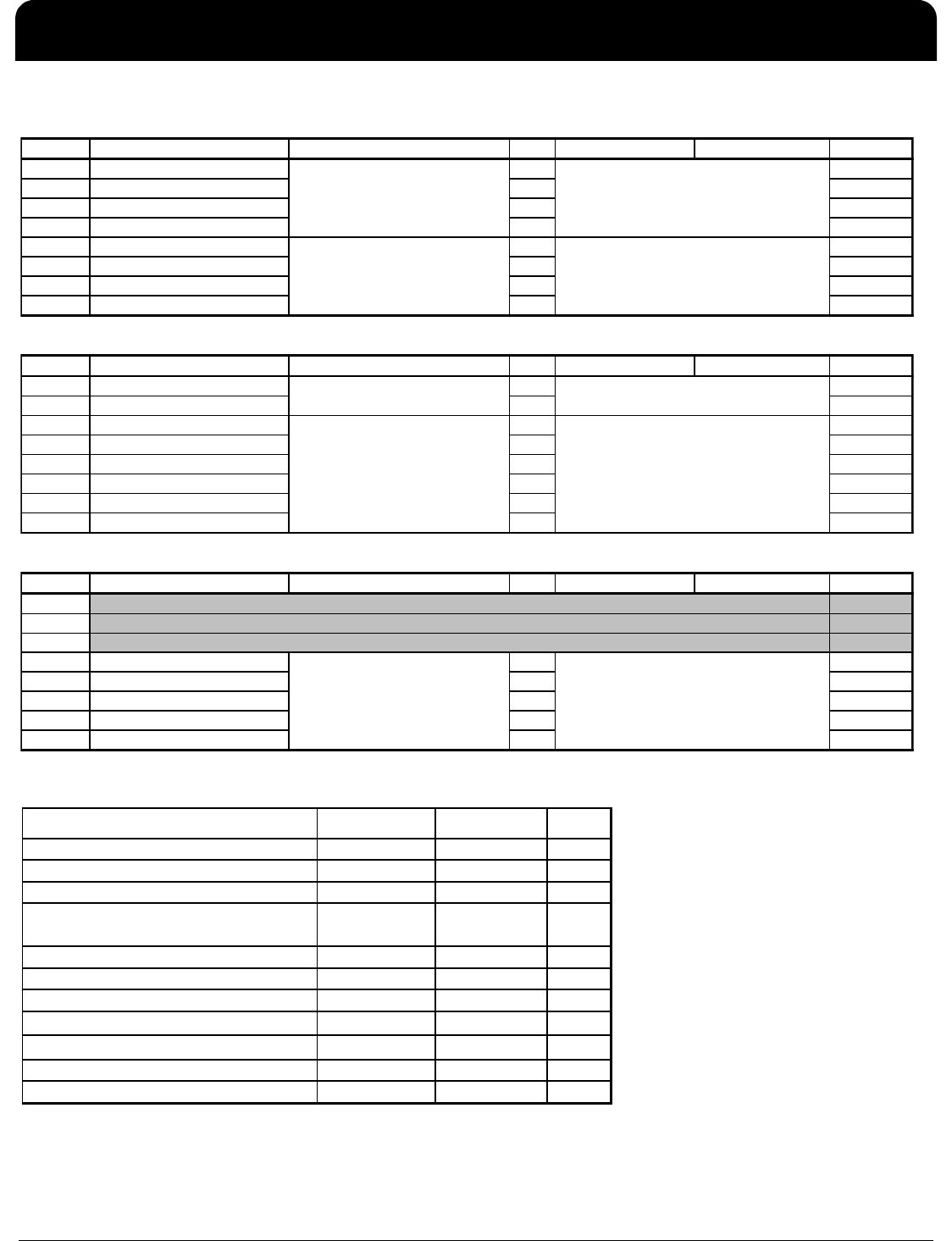
SMBus Table: Output Enable Register
Byte 0 Name Control Function Type 0 1 Default
Bit 7
1
Bit 6
1
Bit 5
1
Bit 4
1
Bit 3
1
Bit 2
DIF OE1 Output Enable RW Low/Low Enabled 1
Bit 1
DIF OE0 Output Enable RW Low/Low Enabled 1
Bit 0
1
SMBus Table: SS Readback and Vhigh Control Register
Byte 1 Name Control Function Type 0 1 Default
Bit 7
SSENRB1 SS Enable Readback Bit1
R
Latch
Bit 6
SSENRB1 SS Enable Readback Bit0
R
Latch
Bit 5
SSEN_SWCNTRL Enable SW control of SS RW SS control locked
Values in B1[4:3]
control SS amount.
0
Bit 4
SSENSW1 SS Enable Software Ctl Bit1
RW
1
0
Bit 3
SSENSW0 SS Enable Software Ctl Bit0
RW
1
0
Bit 2
1
Bit 1
AMPLITUDE 1 RW 00 = 0.6V 01 = 0.7V 1
Bit 0
AMPLITUDE 0 RW 10= 0.8V 11 = 0.9V 0
1. B1[5] must be set to a 1 for these bits to have any effect on the part.
SMBus Table: DIF Slew Rate Control Register
Byte 2 Name Control Function Type 0 1 Default
Bit 7
1
Bit 6
1
Bit 5
1
Bit 4
1
Bit 3
1
Bit 2
SLEWRATESEL DIF1 Adjust Slew Rate of DIF1 RW 2.0V/ns 3.0V/ns 1
Bit 1
SLEWRATESEL DIF0 Adjust Slew Rate of DIF0 RW 2.0V/ns 3.0V/ns 1
Bit 0
1
SMBus Table: REF Control Register
Byte 3 Name Control Function Type 0 1 Default
Bit 7
RW 00 = Slowest 01 = Slow 0
Bit 6
RW 10 = Fast 11 = Faster 1
Bit 5
REF Power Down Function Wake-on-Lan Enable for REF RW
REF does not run in
Power Down
REF runs in Power
Down
0
Bit 4
REF OE REF Output Enable RW Low Enabled 1
Bit 3
1
Bit 2
1
Bit 1
1
Bit 0
1
Byte 4 is reserved and reads back 'hFF'.
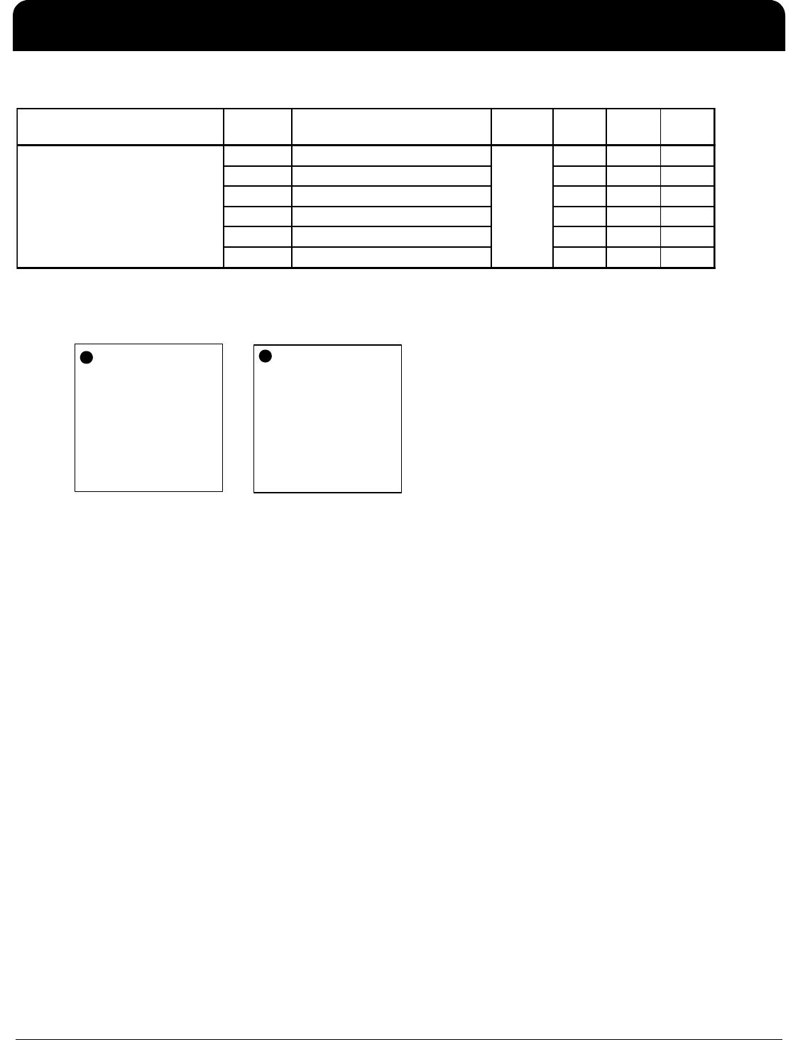
Reserved
Reserved
Slew Rate Control
00' = SS Off, '01' = -0.25% SS,
'10' = Reserved, '11'= -0.5% SS
00' for SS_EN_tri = 0, '01' for SS_EN_tri
= 'M', '11 for SS_EN_tri = '1'
REF
Reserved
Controls Output Amplitude
Reserved
Reserved
Reserved
Reserved
Reserved
Reserved
Reserved
Reserved
Reserved
Reserved
Reserved
Reserved
Reserved
Reserved
9FGV0241
2-OUTPUT VERY LOW POWER PCIE GEN1/2/3 CLOCK GENERATOR
IDT®
2-OUTPUT VERY LOW POWER PCIE GEN1/2/3 CLOCK GENERATOR 11
9FGV0241 OCTOBER 18, 2016
Recommended Crystal Characteristics (3225 package)
SMBus Table: Revision and Vendor ID Register
Byte 5 Name Control Function Type 0 1 Default
Bit 7
RID3
R
0
Bit 6
RID2
R
0
Bit 5
RID1
R
0
Bit 4
RID0
R
0
Bit 3
VID3
R
0
Bit 2
VID2
R
0
Bit 1
VID1
R
0
Bit 0
VID0
R
1
SMBus Table: Device Type/Device ID
Byte 6 Name Control Function Type 0 1 Default
Bit 7
Device Type1
R
0
Bit 6
Device Type0
R
0
Bit 5
Device ID5
R
0
Bit 4
Device ID4
R
0
Bit 3
Device ID3
R
0
Bit 2
Device ID2
R
0
Bit 1
Device ID1
R
1
Bit 0
Device ID0
R
0
SMBus Table: Byte Count Register
Byte 7 Name Control Function Type 0 1 Default
Bit 7
0
Bit 6
0
Bit 5
0
Bit 4
BC4 RW 0
Bit 3
BC3 RW 1
Bit 2
BC2 RW 0
Bit 1
BC1 RW 0
Bit 0
BC0 RW 0
A rev = 0000
Byte Count Programming
Writing to this register will configure how
many bytes will be read back, default is
= 8 bytes.
Device Type
Revision ID
Reserved
0001 = IDT
00010 binary or 02 hex
00 = FGV, 01 = DBV,
10 = DMV, 11= Reserved
Device ID
Reserved
VENDOR ID
Reserved
PARAMETER VALUE UNITS NOTES
Frequency 25 MHz 1
Resonance Mode Fundamental
-
1
Frequency Tolerance @ 25°C
±
20 PPM Max 1
Frequency Stability, ref @ 25°C Over
Operating Temperature Range
±
20 PPM Max 1
Temperature Range (commerical) 0~70 °
C
1
Temperature Range (industrial) -40~85 °
C
2
Equivalent Series Resistance (ESR) 50
Max 1
Shunt Capacitance (C
O
)7pF Max1
Load Capacitance (C
L
)8pF Max1
Drive Level 0.3 mW Max 1
Aging per year
±5
PPM Max 1
Notes:
1. FOX 603-25-150.
2. For I-temp, FOX 603-25-261.
9FGV0241
2-OUTPUT VERY LOW POWER PCIE GEN1/2/3 CLOCK GENERATOR
IDT®
2-OUTPUT VERY LOW POWER PCIE GEN1/2/3 CLOCK GENERATOR 12
9FGV0241 OCTOBER 18, 2016
Thermal Characteristics
Marking Diagrams
Notes:
1. ‘LOT’ is the lot number.
2. ‘YYWW’ is the last two digits of the year and week that the part was assembled.
3. ‘L’ denotes RoHS compliant package.
4. ‘I’ denotes industrial temperature grade.
PARAMETER SYMBOL CONDITIONS PKG
TYP
VALUE
UNITS NOTES
θ
JC
Junction to Case 62 °
C/W
1
θ
Jb
Junction to Base 5.4 °
C/W
1
θ
JA0
Junction to Air, still air 50 °
C/W
1
θ
JA1
Junction to Air, 1 m/s air flow 43 °
C/W
1
θ
JA3
Junction to Air, 3 m/s air flow 39 °
C/W
1
θ
JA5
Junction to Air, 5 m/s air flow 38 °
C/W
1
1
ePad soldered to board
Thermal Resistance
NLG20
NLG24
LOT
241AL
YYWW
LOT
241AIL
YYWW

9FGV0241AKLF

Mfr. #:
Manufacturer:
IDT
Description:
Clock Generators & Support Products PCIe CLOCK GENERATOR GEN 1/2/3, 2 OUT
Lifecycle:
New from this manufacturer.
Delivery:
DHL FedEx Ups TNT EMS
Payment:
T/T Paypal Visa MoneyGram Western Union

Products related to this Datasheet