9FGV0241
2-OUTPUT VERY LOW POWER PCIE GEN1/2/3 CLOCK GENERATOR
IDT®
2-OUTPUT VERY LOW POWER PCIE GEN1/2/3 CLOCK GENERATOR 4
9FGV0241 OCTOBER 18, 2016
Test Loads
Alternate Terminations
Rs
Rs
Low-Power HCSL Differential Output Test Load
2pF 2pF
5 inches
Zo=100ohm
Device
Rs
Device
Rs
Zo
Driving LVDS
Cc
Cc
R7a R7b
R8a
R8b
3.3V
LVDS Clock
input
Driving LVDS inputs with the 9FGV0241
Receiver has
termination
Receiver does not
have termination
R7a, R7b 10K ohm 140 ohm
R8a, R8b 5.6K ohm 75 ohm
Cc 0.1 uF 0.1 uF
Vcm 1.2 volts 1.2 volts
Component
Value
Note
9FGV0241
2-OUTPUT VERY LOW POWER PCIE GEN1/2/3 CLOCK GENERATOR
IDT®
2-OUTPUT VERY LOW POWER PCIE GEN1/2/3 CLOCK GENERATOR 5
9FGV0241 OCTOBER 18, 2016
Absolute Maximum Ratings
Stresses above the ratings listed below can cause permanent damage to the 9FGV0241. These ratings, which are standard
values for IDT commercially rated parts, are stress ratings only. Functional operation of the device at these or any other
conditions above those indicated in the operational sections of the specifications is not implied. Exposure to absolute
maximum rating conditions for extended periods can affect product reliability. Electrical parameters are guaranteed only over
the recommended operating temperature range.
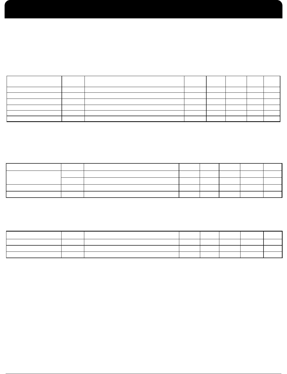
Electrical Characteristics–Current Consumption
Electrical Characteristics–Output Duty Cycle, Jitter, and Skew Characteristics
PARAMETER SYMBOL CONDITIONS
MIN TYP MAX
UNITS NOTES
1.8V Supply Voltage VDDxx Applies to All VDD pins -0.5 2.5 V 1,2
Input Voltage V
IN
-0.5 V
DD
+0.3V V 1, 3
Input High Voltage, SMBus V
IHSMB
SMBus clock and data pins 3.6V V 1
Storage Temperature Ts -65 150 °C
1
Junction Temperature Tj 125 °C 1
Input ESD protection
ESD prot Human Body Model 2000 V 1
1
Guaranteed by design and characterization, not 100% tested in production.
2
Operation under these conditions is neither implied nor guaranteed.
3
Not to exceed 2.5V.
TA = T
COM
or T
IND;
Supply Voltage per VDD of normal operation conditions, See Test Loads for Loading Conditions
PARAMETER SYMBOL CONDITIONS MIN TYP MAX UNITS NOTES
I
DDAOP
VDDA, PLL Mode, All outputs active @100MHz 7 8 mA 1
I
DDOP
VDD, All outputs active @100MHz 15 18 mA 1
Suspend Supply Current I
DDSUSP
VDDxxx, PD# = 0, Wake-On-LAN enabled 6 8 mA 1
Powerdown Current I
DDPD
PD#=0 0.6 1 mA 1, 2
1
Guaranteed by desi
g
n and characterization, not 100% tested in production.
2
Assumin
g
REF is not runnin
g
in power down state
Operating Supply Current
TA = T
COM
or T
IND;
Supply Voltage per VDD of normal operation conditions, See Test Loads for Loading Conditions
PARAMETER SYMBOL CONDITIONS MIN TYP MAX UNITS NOTES
Duty Cycle t
D
C
Measured differentially, PLL Mode 45 50 55 % 1
Skew, Output to Output t
sk3
V
T
= 50% 34 50 ps 1
Jitter, Cycle to cycle t
jcyc-cyc
PLL mode 14 50 ps 1,2
1
Guaranteed by design and characterization, not 100% tested in production.
2
Measured from differential waveform
9FGV0241
2-OUTPUT VERY LOW POWER PCIE GEN1/2/3 CLOCK GENERATOR
IDT®
2-OUTPUT VERY LOW POWER PCIE GEN1/2/3 CLOCK GENERATOR 6
9FGV0241 OCTOBER 18, 2016
Electrical Characteristics–Input/Supply/Common Parameters–Normal Operating
Conditions
TA = T
COM
or T
IND;
Supply Voltage per VDD of normal operation conditions, See Test Loads for Loading Conditions
PARAMETER SYMBOL CONDITIONS MIN TYP MAX UNITS NOTES
1.8V Supply Voltage VDD
Supply voltage for core, analog and single-ended
LVCMOS outputs
1.7 1.8 1.9 V 1
T
COM
Commmercial range 0 25 70 °C 1
T
IND
Industrial range -40 25 85 °C 1
Input High Voltage V
IH
Single-ended inputs, except SMBus 0.75 V
DD
V
DD
+ 0.3 V 1
Input Mid Voltage V
IM
Single-ended tri-level inputs ('_tri' suffix, if present) 0.4 V
DD
0.6 V
DD
V1
Input Low Voltage V
IL
Single-ended inputs, except SMBus -0.3 0.25 V
DD
V1
Schmitt Trigger Postive
Goin
g
Threshold Volta
g
e
V
T+
Single-ended inputs, where indicated 0.4 V
DD
0.7 V
DD
V1
Schmitt Trigger Negative
Going Threshold Voltage
V
T-
Single-ended inputs, where indicated 0.1 V
DD
0.4 V
DD
V1
Hysteresis Voltage V
H
V
T+
- V
T-
0.1 V
DD
0.4 V
DD
V1
Output High Voltage V
IH
Single-ended outputs, except SMBus. I
OH
= -2mA V
DD
-0.45 V 1
Output Low Voltage V
IL
Single-ended outputs, except SMBus. I
OL
= -2mA 0.45 V 1
I
IN
Single-ended inputs, V
IN
= GND, V
IN
= VDD -5 5 uA 1
I
INP
Single-ended inputs
V
IN
= 0 V; Inputs with internal pull-up resistors
V
IN
= VDD; Inputs with internal pull-down resistors
-200 200 uA 1
Input Frequency F
in
XTAL, or X1 input 23 25 27 MHz
1
Pin Inductance L
p
in
7nH1
C
IN
Logic Inputs, except DIF_IN 1.5 5 pF 1
C
OUT
Output pin capacitance 6 pF 1
Clk Stabilization T
STAB
From V
DD
Power-Up and after input clock
stabilization or de-assertion of PD# to 1st clock
0.4 1.8 ms 1,2
SS Modulation Frequency f
MOD
Allowable Frequency
(Triangular Modulation)
31 31.6 32 kHz 1
OE# Latency t
LATOE#
DIF start after OE# assertion
DIF stop after OE# deassertion
123clocks1,3
Tdrive_PD# t
DRVPD
DIF output enable after
PD# de-assertion
300 us 1,3
Tfall t
F
Fall time of single-ended control inputs 5 ns 1,2
Trise t
R
Rise time of single-ended control inputs 5 ns 1,2
SMBus Input Low Voltage V
ILSMB
V
DDSMB
= 3.3V, see note 4 for V
DDSMB
< 3.3V 0.8 V 1,4
SMBus Input High Voltage V
IHSMB
V
DDSMB
= 3.3V, see note 5 for V
DDSMB
< 3.3V 2.1 3.6 V 1,5
SMBus Output Low Voltage V
OLSMB
@ I
PULLUP
0.4 V 1
SMBus Sink Current I
PULLUP
@ V
OL
4mA1
Nominal Bus Voltage V
DDSMB
1.7 3.6 V 1
SCLK/SDATA Rise Time t
RSMB
(Max VIL - 0.15) to (Min VIH + 0.15) 1000 ns 1
SCLK/SDATA Fall Time t
FSMB
(Min VIH + 0.15) to (Max VIL - 0.15) 300 ns 1
SMBus Operating
Frequency
f
MAXSMB
Maximum SMBus operating frequency 400 kHz 1
1
Guaranteed by desi
g
n and characterization, not 100% tested in production.
2
Control input must be monotonic from 20% to 80% of input swing.
Capacitance
3
Time from deassertion until outputs are >200 mV
4
For V
DDSMB
< 3.3V, V
ILSMB
<= 0.35V
DDSMB
Input Current
5
For V
DDSMB
< 3.3V, V
IHSMB
>= 0.65V
DDSMB
Ambient Operating
Temperature

9FGV0241AKLF

Mfr. #:
Manufacturer:
IDT
Description:
Clock Generators & Support Products PCIe CLOCK GENERATOR GEN 1/2/3, 2 OUT
Lifecycle:
New from this manufacturer.
Delivery:
DHL FedEx Ups TNT EMS
Payment:
T/T Paypal Visa MoneyGram Western Union

Products related to this Datasheet