ADMV1012 Data Sheet
Rev. A | Page 2 of 19
TABLE OF CONTENTS
Features .............................................................................................. 1
Applications ....................................................................................... 1
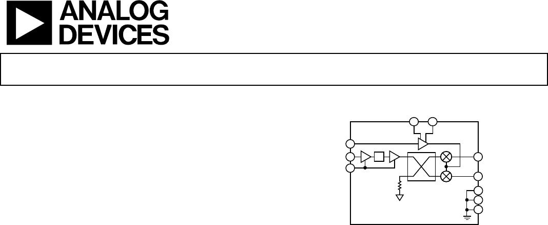
Functional Block Diagram .............................................................. 1
General Description ......................................................................... 1
Revision History ............................................................................... 2
Specifications ..................................................................................... 3
Absolute Maximum Ratings ............................................................ 4
Thermal Resistance ...................................................................... 4
ESD Caution .................................................................................. 4
Pin Configuration and Function Descriptions ............................. 5
Typical Performance Characteristics ............................................. 6
Upper Sideband (Low-Side LO) ................................................. 6
Lower Sideband (High-Side LO) ................................................ 8
IF Bandwidth .............................................................................. 10
Leakage Performance ................................................................. 11
Return Loss Performance .......................................................... 12
Spurious Performance ............................................................... 13
M × N Spurious Performance for LO = 0 dBm ...................... 13
Theory of Operation ...................................................................... 14
LO Driver Amplifier .................................................................. 14
Mixer ............................................................................................ 14
LNA .............................................................................................. 14
Applications Information .............................................................. 15
Typical Application Circuit ....................................................... 15
Evaluation Board Information ................................................. 16
Bill of Materials ........................................................................... 18
Outline Dimensions ....................................................................... 19
Ordering Guide .......................................................................... 19
REVISION HISTORY
2/2018—Rev. 0 to Rev. A
Changes to Features Section, General Description Section, and
Figure 1 .............................................................................................. 1
Changes to Table 1 ............................................................................ 3
Changes to Table 2 ............................................................................ 4
Added Thermal Resistance Section and Table 3; Renumbered
Sequentially ....................................................................................... 4
Changes to Figure 2 and Table 4 ..................................................... 5
Changes to Figure 3 and Figure 6 ................................................... 6
Changes to Figure 12 ........................................................................ 7
Changes to Figure 24, Figure 25, and Figure 26 ......................... 10
Changes to Figure 27 through Figure 30 ..................................... 11
Changed M × N Spurious Performance for LO = 4 dBm Section
to M × N Spurious Performance for LO = 0 dBm Section ....... 13
Changes to M × N Spurious Performance for LO = 0 dBm
Sec tion .............................................................................................. 13
Changes to LO Driver Amplifier Section .................................... 14
Changes to Applications Information Section and Figure 34 ........ 15
Changes to Power-On Sequence Section .................................... 16
Changes to Figure 37 ...................................................................... 17
Changes to Table 6 .......................................................................... 18
Changes to Ordering Guide .......................................................... 19
10/2017—Revision 0: Initial Version