ADMV1012 Data Sheet
Rev. A | Page 4 of 19
ABSOLUTE MAXIMUM RATINGS
Table 2.
Parameter Rating
Supply Voltage
VDLO 4 V
VGRF 0 V
VDRF − VGRF
1
6 V
Input Power
RF 15 dBm
LO 15 dBm
Maximum Junction Temperature 175°C
Maximum Power Dissipation 2 W
Lifetime at Maximum Junction Temperature (T
J
) >1 million hours
Operating Temperature Range −40°C to +85°C
Storage Temperature Range −65°C to +150°C
Lead Temperature (Soldering 60 sec) 260°C
Moisture Sensitivity Level (MSL) Rating MSL3
Electrostatic Discharge (ESD) Sensitivity
Human Body Model (HBM) 750 V
Field Induced Charged Device Model
(FICDM)
500 V
1
The maximum VDRF voltage and the minimum VGRF voltage is determined
by this difference. If a maximum VDRF voltage of +4 V is required, then the
minimum VGRF voltage is −2 V.
Stresses at or above those listed under Absolute Maximum
Ratings may cause permanent damage to the product. This is a
stress rating only; functional operation of the product at these
or any other conditions above those indicated in the operational
section of this specification is not implied. Operation beyond
the maximum operating conditions for extended periods may
affect product reliability.
THERMAL RESISTANCE
Thermal performance is directly linked to printed circuit board
(PCB) design and operating environment. Careful attention to
PCB thermal design is required.
θ
JA
is thermal resistance, junction to ambient (°C/W), and θ
JC
is
thermal resistance, junction to case (°C/W).
Table 3. Thermal Resistance
Package Type θ
JA
1
θ
JC
Unit
E-32-1 33.4 34 °C/W
1
See JEDEC standard JESD51-2 for additional information on optimizing the
thermal impedance (PCB with 3 × 3 vias).
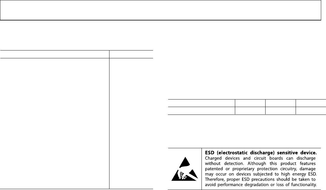
ESD CAUTION
Data Sheet ADMV1012
Rev. A | Page 5 of 19
PIN CONFIGURATION AND FUNCTION DESCRIPTIONS
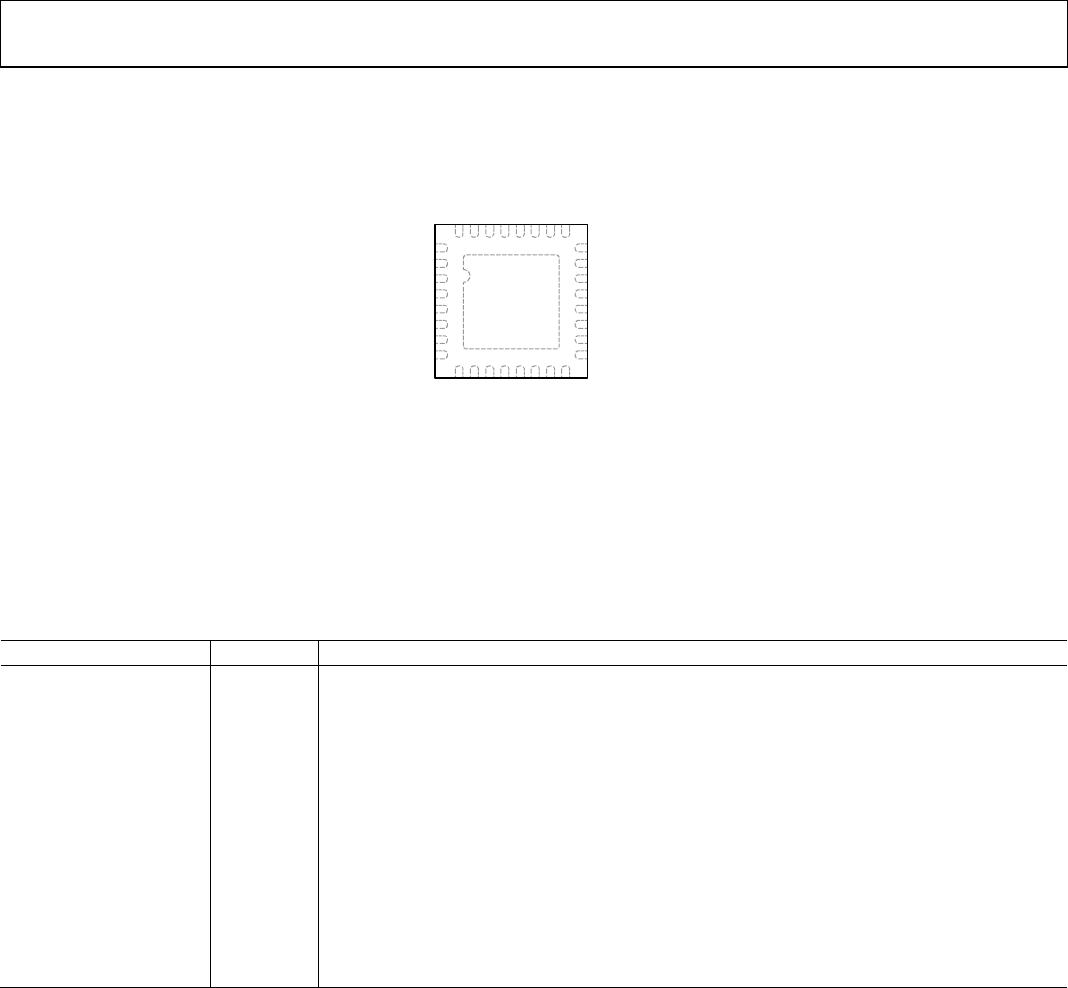
24 NIC
23
NIC
22
IF1
21 NIC
20 IF2
19
NIC
18 NIC
17 NIC
1
2
3
4
5
6
7
8
NIC
GND
RFIN
GND
NIC
NIC
NIC
NIC
9
10
11
12
13
14
15
16
NIC
LOIN
GND
NIC
NIC
NIC
VDLO
NIC
32
31
30
29
28
27
26
25
NIC
VGRF
NIC
NIC
NIC
VDRF
NIC
NIC
ADMV1012
TOP VIEW
(Not to Scale)
16349-002
NOTES
1. NIC = NOT INTERNALLY CONNECTED. IT IS
RECOMMENDED TO GROUND THESE PINS
ON THE PCB.
2. EXPOSED PAD. THE EXPOSED PAD MUST BE
CONNECTED TO GND. GOOD RF AND THERMAL
GROUNDING IS RECOMMENDED.
Figure 2. Pin Configuration
Table 4. Pin Function Descriptions
Pin No. Mnemonic Description
1, 5 to 9, 12 to 14, 16 to 19,
21, 23 to 26, 28 to 30, 32
NIC Not Internally Connected. It is recommended to ground these pins on the PCB.
2, 4, 11 GND Ground.
3 RFIN RF Input. This pin is ac-coupled internally and matched to 50single ended.
10 LOIN LO Input. This pin is ac-coupled internally and matched to 50 Ω single ended.
15
VDLO
Power Supply Voltage for the LO Amplifier. Refer to the Applications Information section for the
required external components and biasing.
20, 22 IF2, IF1 Quadrature IF Outputs. Matched to 50 Ω and ac coupled. No external dc block is required.
27 VDRF Power Supply Voltage for the RF Amplifier. Refer to the Applications Information section for the
required external components and biasing.
31 VGRF Power Supply Gate Voltage for the RF Amplifier. Refer to the Applications Information section for
the required external components and biasing.
EPAD Exposed Pad. The exposed pad must be connected to GND. Good RF and thermal grounding is
recommended.
ADMV1012 Data Sheet
Rev. A | Page 6 of 19
TYPICAL PERFORMANCE CHARACTERISTICS
UPPER SIDEBAND (LOW-SIDE LO)
Data taken at VDRF = 3 V, V D L O = 3 V, IDRF = 68 mA, LO = 4 dBm LO +4 dBm, −40°C ≤ T
A
+85°C, with Mini-Circuits QCN-45+,
power splitter as upper sideband (low-side LO), unless otherwise noted.
20
0
2
4
6
8
10
12
14
16
18
20.0 20.5 21.0 21.5 22.0 22.5 23.0 23.5 24.0
CONVERSION GAIN (dB)
RF FREQUENCY (GHz)
+85°C, 3.5GHz IF
+25°C, 3.5GHz IF
–40°C, 3.5GHz IF
+85°C, 3.0GHz IF
+25°C, 3.0GHz IF
–40°C, 3.0GHz IF
+85°C, 2.5GHz IF
+25°C, 2.5GHz IF
–40°C , 2.5GHz IF
16349-003
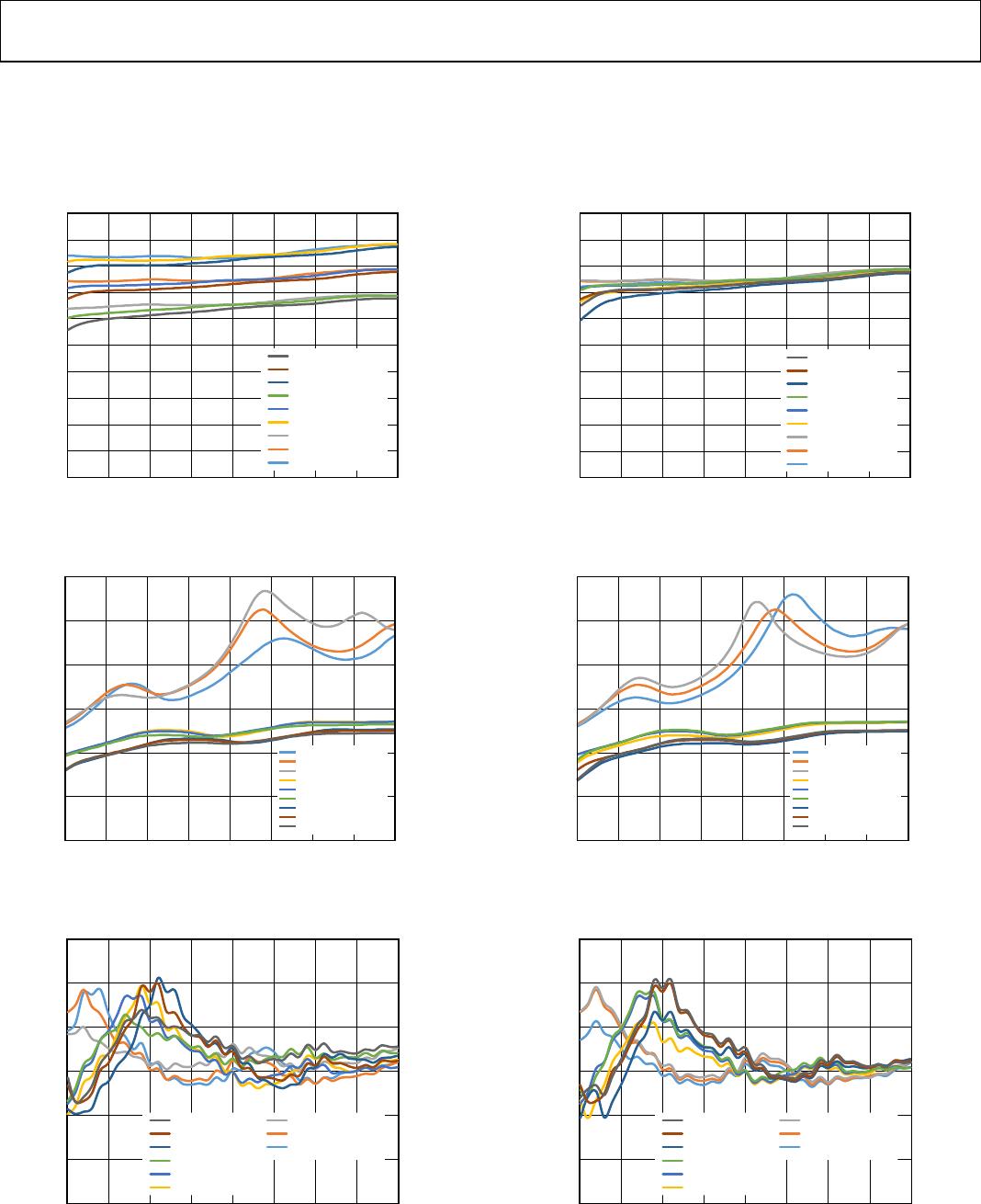
Figure 3. Conversion Gain vs. RF Frequency at Various Temperatures and
Various IF Frequencies
0
10
20
30
40
50
60
20.0 20.5
21.0 21.5 22.0 22.5 23.0 23.5
24.0
IMAGE REJECTI
ON (dBc)
RF FREQUENCY (GHz)
–40°C, 2.5G
Hz I
F
+25°C, 2.5
GHz I
F
+85°C
, 2.5GHz IF
–40°C, 3.0GHz IF
+25°C, 3.0GHz I
F
+85°C,
3.0GHz
IF
–40°C
, 3.5GH
z IF
+25°C,
3.5GHz
IF
+85°C,
3.5GHz I
F
16349-004
Figure 4. Image Rejection vs. RF Frequency at Various Temperatures and
Various IF Frequencies
12
0
2
4
6
8
10
20.0 20.5 21.0 21.5 22.0 22.5 23.0 23.5 24.0
INPUT IP3 (dBm)
RF FREQUENCY (GHz)
+85°C, 3.5GHz IF
+25°C, 3.5GHz IF
–40°C, 3.5GHz IF
+85°C, 3.0GHz IF
+25°C, 3.0GHz IF
–40°C, 3.0GHz IF
+85°C, 2.5GHz IF
+25°C, 2.5GHz IF
–40°C, 2.5GHz IF
16349-005
Figure 5. Input IP3 vs. RF Frequency at Various Temperatures and Various
IF Frequencies
20
18
0
2
4
6
8
10
12
14
16
20.0 20.5 21.0
21.5 22.0 22.5 23.0 23.5 24.0
CONVERSION GAIN (dB)
RF FREQUENCY (GHz)
+4°C, 3.5GHz IF
0°C, 3.5GHz IF
–4°C, 3.5GHz IF
+4°C, 3.0GHz IF
0°C, 3.0GHz IF
–4°C, 3.0GHz IF
+4°C, 2.5GHz IF
0°C, 2.5GHz IF
–4°C, 2.5GHz IF
16349-006
Figure 6. Conversion Gain vs. RF Frequency at Various LO Powers and
Various IF Frequencies
0
10
20
30
40
50
60
20.0 20.5
21.0
21.5 22.0 22.5 23.0 23.5 24.0
IMAGE REJECTION (
dBc)
RF FREQUENCY
(GH
z)
16349-007
–4
d
B, 2.5
GHz IF
0
dB,
2.5G
H
z I
F
+4
d
B,
2.5G
H
z
I
F
–4dB,
3.0GH
z I
F
0
dB, 3.0
GHz
IF
+4
d
B,
3.0G
H
z I
F
–4dB,
3.5GHz
IF
0dB, 3.5GHz IF
+4dB, 3.5GHz IF
Figure 7. Image Rejection vs. RF Frequency at Various LO Powers and
Various IF Frequencies
12
0
2
4
6
8
10
20.0 20.5 21.0 21.5 22.0 22.5 23.0 23.5 24.0
INPUT IP3 (dBm)
RF FREQUENCY (GHz)
+4dB, 3.5GHz IF
0dB, 3.5GHz IF
–4dB, 3.5GHz IF
+4dB, 3.0GHz IF
0dB, 3.0GHz IF
–4dB, 3.0GHz IF
+4dB, 2.5GHz IF
0dB, 2.5GHz IF
–4dB, 2.5GHz IF
16349-008
Figure 8. Input IP3 vs. RF Frequency at Various LO Powers and Various IF
Frequencies

ADMV1012AEZ

Mfr. #:
Manufacturer:
Analog Devices Inc.
Description:
Up-Down Converters 18/23GHz GaAs D/C
Lifecycle:
New from this manufacturer.
Delivery:
DHL FedEx Ups TNT EMS
Payment:
T/T Paypal Visa MoneyGram Western Union

Products related to this Datasheet