Data Sheet ADMV1012
Rev. A | Page 13 of 19
SPURIOUS PERFORMANCE
Data taken at VDRF = 3 V, VDLO = 3 V, IDRF = 68 mA, LO =
0 dBm, and −40°C ≤ T
A
≤ +85°C with a Mini-Circuits QCN-45+,
power splitter, unless otherwise noted.
Table 5. LO Harmonic Leakage at IF Output
Frequency
LO Frequency (MHz) 1.0 2.0 3.0 4.0
7000 −48 −65 −42 −57
8500 −47 −64 −57 −64
9000 −50 −51 −51 −61
10,000 −49 −40 −52 −61
11,000 −49 −47 −61 N/A
12,000 −58 −46 −56 N/A
13,000 −54 −42 −59 N/A
13,500 −55 −40 N/A N/A
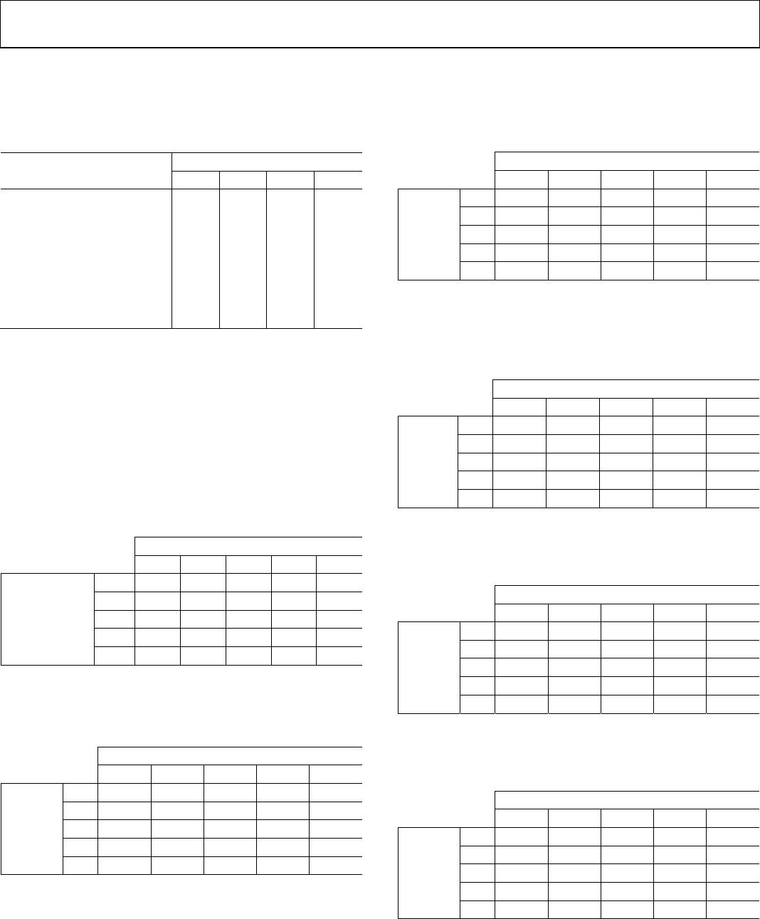
M × N SPURIOUS PERFORMANCE FOR LO = 0 dBm
Mixer spurious products are measured in dBc from the IF
output power level. Spurious values are measured using the
following equation: (M × RF)+ (N × LO). N/A means not
applicable. The frequencies are referred from the frequencies
applied to the pin of the ADMV1012.
Lower Sideband
IF = 2.8 GHz
RF = 18000 MHz at −20 dBm and LO = 10400 MHz at 4 dBm.
All values in dBc below IF power level. N/A means not applicable.
N × LO
0 1 2 3 4
M × RF
−2
N/A N/A N/A N/A −58.6
−1
N/A N/A 0 −68.5 −71.1
0
N/A −42 −38.4 −52.2 −53.2
1
−49.1 −70.2 −65.7 −67.9 N/A
2
−66.5 −74.4 N/A N/A N/A
IF = 3.3 GHz
RF = 18000 MHz at RF power of −20 dBm, and LO = 10650 MHz
at LO power of 4 dBm. All values in dBc below IF power level.
N/A means not applicable.
N × LO
0 1 2 3 4
M × RF
−2
N/A N/A N/A N/A −56
−1
N/A N/A 0 −72.5 −83.9
0
N/A −42.3 −44.7 −54.1 −56.9
1
−48.8 −68.3 −69.5 −63.4 N/A
2
−71.7 −65.8 N/A N/A N/A
IF = 3.5 GHz
RF = 18000 MHz at RF power of −20 dBm, and LO = 10750 MHz
at LO power of 4 dBm. All values in dBc below IF power level.
N/A means not applicable.
N × LO
0 1 2 3 4
M × RF
−2
N/A N/A N/A N/A −57.5
−1
N/A N/A 0 −76.6 −74.2
0
N/A −42.7 −33.4 −47.2 −46.2
1
−48.2 −74.5 −83.8 N/A N/A
2
−77.2 −59.9 N/A N/A N/A
Upper Sideband
IF = 2.8 GHz
RF = 23000 MHz at RF power of −20 dBm, and LO = 10100 MHz
at LO power of 4 dBm. All values in dBc below IF power level.
N/A means not applicable.
N × LO
0 1 2 3 4
M ×RF
−2
N/A N/A N/A N/A −56.4
−1
N/A N/A 0 −62.6 −72.3
0
N/A −39.9 −40.2 −46.9 −47
1
−53.2 −77.8 −64.9 N/A N/A
2
−60.9 N/A N/A N/A N/A
IF = 3.3 GHz
RF = 23000 MHz at RF power of −20 dBm, and LO = 9850 MHz
at LO power of 4 dBm. All values in dBc below IF power level.
N/A means not applicable.
N × LO
0 1 2 3 4
M × RF
−2
N/A N/A N/A N/A −61.5
−1
N/A N/A 0 −53.8 −69
0
N/A −40.6 −42 −44.2 −56.5
1
−52.9 −99.8 −65.3 N/A N/A
2
−74.9 N/A N/A N/A N/A
IF = 3.5 GHz
RF = 23000 MHz at RF power of −20 dBm, and LO = 9750 MHz
at LO power of 4 dBm. All values in dBc below IF power level.
N/A means not applicable.
N × LO
0 1 2 3 4
M × RF
−2
N/A N/A N/A N/A −67.6
−1
N/A N/A 0 −50.1 −63.9
0
N/A −41.5 −40.8 −47.4 −64.8
1
−53.6 −68.7 −72.2 N/A N/A
2
−70.7 N/A N/A N/A N/A
ADMV1012 Data Sheet
Rev. A | Page 14 of 19
THEORY OF OPERATION
The ADMV1012 is a compact GaAs, MMIC, double sideband
(DSB) downconverter in a RoHS compliant package optimized
for both upper sideband and lower sideband point to point
microwave radio applications operating in the 17.5 GHz to
24 GHz input frequency range. The ADMV1012 supports
LO input frequencies of 7 GHz to 13.5 GHz and IF output
frequencies of 2.5 GHz to 3.5 GHz.
The ADMV1012 uses a RF LNA followed by an I/Q double
balanced mixer, where a driver amplifier drives the LO (see
Figure 1). This combination of design, process, and packaging
technology allows the functions of these subsystems to be
integrated into a single die, using mature packaging and
interconnection technologies to provide a high performance,
low cost design with excellent electrical, mechanical, and
thermal properties. In addition, the need for external
components is minimized, optimizing cost and size.
LO DRIVER AMPLIFIER
The LO driver amplifier takes a single LO input and doubles the
frequency and amplifies it to the desired LO signal level for the
mixer to operate optimally. The LO driver amplifier is self
biased, and it requires only a single dc bias voltage (VDLO),
which draws approximately 170 mA at 3 V under the LO drive.
The LO amplitude range of −4 dBm to +4 dBm makes it
compatible with the Analog Devices, Inc., wideband synthesizer
portfolio without the need for an external LO driver amplifier.
MIXER
The mixer is an I/Q double balanced mixer, and this mixer
topology reduces the need for filtering unwanted sideband.
An external 90° hybrid is required to select the upper sideband
of operation. The ADMV1012 has been optimized to work with
the Mini-Circuits QCN-45+ RF 90° hybrid.
LNA
The LNA requires a single dc bias voltage (VDRF) and a single
dc gate bias (VGRF) to operate. Starting at −1.8 V at the gate
supply (VGRF), the LNA is biased at +3 V (VDRF). Then, the
gate bias (VGRF) is varied until the desired LNA bias current
(IDRF) is achieved. The desired LNA bias current is 68 mA at
3 V under small signal conditions.
The typical application circuit (see Figure 34) shows the
necessary external components on the bias lines to eliminate
any undesired stability problems for the RF amplifier and the
LO amplifier.
The ADMV1012 is a much smaller alternative to hybrid style
image reject converter assemblies, and it eliminates the need
for wire bonding by allowing the use of surface-mount
manufacturing assemblies.
The ADMV1012 downconverter comes in a compact, thermally
enhanced, 4.9 mm × 4.9 mm, 32-terminal ceramic leadless chip
carrier (LCC) package. The ADMV1012 operates over the
40°C to +85°C temperature range.
Data Sheet ADMV1012
Rev. A | Page 15 of 19
APPLICATIONS INFORMATION
The evaluation board and typical application circuit are
optimized for low-side LO (upper sideband) performance
with the Mini-Circuit QCN-45+ RF 90° hybrid. Because the
I/Q mixers are double balanced, the ADMV1012 can support IF
frequencies from 3.5 GHz to low frequency.
TYPICAL APPLICATION CIRCUIT
The typical applications circuit is shown in Figure 34. The
application circuit shown has been replicated for the evaluation
board circuit.
16349-049
ADMV1012AEZ
25-146-1000-92
25-146-1000-92
25-146-1000-92
25-146-1000-92
5019
5019 5019
1µF
100pF
0.01µF
100pF
QCN-45+
0.01µF
1µF
100pF
0.01µF
1µF
0Ω
0Ω
DUT
VDLO
VDRF
VGRF
R4
IF_OUTPUT_LSB
C9
C3
LO_INPUT
X1
C7
C10
C5
C13
C12
C11
R1
IF_OUTPUT_USB
RF_INPUT
C8
LO_INPUT
RF_INPUT
VDLO
31
14 27
15
3
PAD
32
30
29
28
26
25
24
23
21
19
18
17
16
13
12
9
8
7
6
5
1
10
22
20
11
4
2
1
11
4 3 2
4 3 2
4 3 2
4 3 2
1
1
1 6
4
2 5
3
1
1
AGND
AGND
AGND
AGND
AGND
AGND
AGND
PORT_1
PORT_2
GND
50Ω _TERM
GND
SUM_PORT
AGND
AGND AGND
AGND
PAD
NIC
VGRF
NIC
NIC
NIC
VDRF
NIC
NIC
NIC
NIC
IF1
NIC
IF2
NIC
NIC
NIC
NIC
VDLO
NIC
NIC
NIC
GND
LOIN
NIC
NIC
NIC
NIC
NIC
GND
RFIN
GND
NIC
Figure 34. Typical Application Circuit

ADMV1012AEZ

Mfr. #:
Manufacturer:
Analog Devices Inc.
Description:
Up-Down Converters 18/23GHz GaAs D/C
Lifecycle:
New from this manufacturer.
Delivery:
DHL FedEx Ups TNT EMS
Payment:
T/T Paypal Visa MoneyGram Western Union

Products related to this Datasheet