ADMV1012 Data Sheet
Rev. A | Page 16 of 19
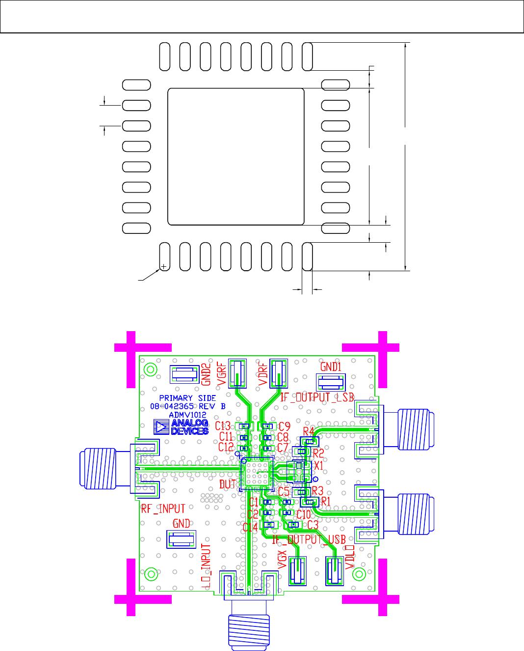
EVALUATION BOARD INFORMATION
The circuit board used in the application must use RF circuit
design techniques. Signal lines must have 50 Ω impedance, and
the package ground leads and exposed pad must be connected
directly to the ground plane similarly to that shown in Figure 35
and Figure 36. Use a sufficient number of via holes to connect
the top and bottom ground planes. The evaluation circuit board
shown in Figure 34 is available from Analog Devices upon request.
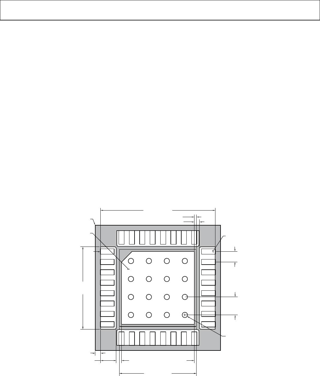
Layout
Solder the exposed pad on the underside of the ADMV1012 to
a low thermal and electrical impedance ground plane. This pad
is typically soldered to an exposed opening in the solder mask
on the evaluation board. Connect these ground vias to all other
ground layers on the evaluation board to maximize heat
dissipation from the device package. Figure 35 shows the PCB
land pattern footprint for the ADMV1012-EVA L Z , and Figure 36
shows the solder paste stencil for the ADMV1012-EVA LZ
evaluation board.
Power-On Sequence
To set up the ADMV1012-EVA L Z , take the following steps:
1. Power up the VGRF with a −1.8 V supply.
2. Power up the VDRF with a 3 V supply.
3. Power up the VDLO with a 3 V supply.
4. Adjust the VGRF supply between −1.8 V to −0.4 V until
IDRF = 68 mA.
5. Connect LOIN to the LO signal generator with an LO
power of between −4 dBm to +4 dBm.
6. For the upper sideband, add a 50 Ω termination to the
IF_OUTPUT_LSB connector. For the lower sideband, add
a 50 Ω termination to the IF_OUTPUT_USB connector.
7. Apply a RF signal to the RF_INPUT and LO_INPUT ports.
Power-Off Sequence
To turn off the ADMV1012-EVA L Z , take the following steps:
1. Turn off the LO and RF signals.
2. Set VGRF to −1.8 V.
3. Set the VDRF supply to 0 V and then turn off the VDRF
supply.
4. Set the VDLO supply to 0 V and then turn off the VDLO
supply.
5. Turn off the VGRF supply.
0.138" SQUARE MASK OPENING
0.02 × 45° CHAMFER FOR PIN 1
0.197"
[0.50]
PAD SIZE
0.026" × 0.010"
0.217" SQUARE
0.004" MASK/METAL OVERLAP
0.010" MINIMUM MASK WIDTH
0.010" REF
0.030"
MASK OPENING
0.156"
MASK
OPENING
PIN 1
GROUND PAD
SOLDER MASK
0.146" SQUARE
GROUND PAD
ø.010"
TYPICAL VIA
ø.034"
TYPICAL
VIA SPACING
16349-050
Figure 35. PCB Land Pattern Footprint of the ADMV1012-EVALZ