ADE7769
Rev. A | Page 9 of 20
–0.5
–0.4
–0.3
–0.2
–0.1
0
0.1
0.2
0.3
0.4
0.5
ERROR (% of Reading)
FREQUENCY (Hz)
5045 55 60 65
05332-018
PF = 0.5 IND
PF = 0.5 CAP
PF = 1
Figure 9. Error as a % of Reading over Input Frequency
–1.0
–0.8
–0.6
–0.4
–0.2
0
ERROR (% of Reading)
0.2
0.4
0.6
05332-023
CURRENT CHANNEL (% of Full Scale)
0.1 101 100
0.8
1.0
5.25V
5V
4.75V
PF = 1
ON-CHIP REFERENCE
Figure 10. PSR with On-Chip Reference, PF = 1
–1.0
–0.8
–0.6
–0.4
–0.2
0
ERROR (% of Reading)
0.2
0.4
0.6
05332-024
CURRENT CHANNEL (% of Full Scale)
0.1 101 100
0.8
1.0
5.25V
5V
4.75V
PF = 1
EXTERNAL REFERENCE
Figure 11. PSR with External Reference, PF = 1
40
FREQUENCY
CHANNEL V1 OFFSET (mV)
05332-025
543210123456789
EXTERNAL REFERENCE
TEMPERATURE = 25°C
0
10
20
30
DISTRIBUTION CHARACTERISTICS
MEAN = 2.247828
SDs = 1.367176
MIN = –2.09932
MAX = +5.28288
NO. OF POINTS = 100
Figure 12. Channel V1 Offset Distribution
0
10
20
30
40
50
FREQUENCY
CHANNEL V2 OFFSET (mV)
05332-026
12108642024681012
EXTERNAL REFERENCE
TEMPERATURE = 25°C
DISTRIBUTION CHARACTERISTICS
MEAN = –1.563484
SDs = 2.040699
MIN = –6.82969
MAX = +2.6119
NO. OF POINTS = 100
Figure 13. Channel V2 Offset Distribution
–10 –8 –6 –4 –2 0 2 4 6 8 10 12
0
200
400
600
800
1000
FREQUENCY
DEVIATION FROM MEAN (%)
05332-027
EXTERNAL REFERENCE
TEMPERATURE = 25°C
DISTRIBUTION CHARACTERISTICS
MEAN = 0%
SDs = 1.55%
MIN = –11.79%
MAX = +6.08%
NO. OF POINTS = 3387
Figure 14. Part-to-Part CF Deviation from Mean
ADE7769
Rev. A | Page 10 of 20
FUNCTIONAL DESCRIPTION
THEORY OF OPERATION
The two ADCs in the ADE7769 digitize the voltage signals from
the current and voltage sensors. These ADCs are 16-bit Σ-Δs
with an oversampling rate of 450 kHz. This analog input
structure greatly simplifies sensor interfacing by providing a
wide dynamic range for direct connection to the sensor and by
simplifying the antialiasing filter design. A high-pass filter in
the current channel removes any dc component from the
current signal. This eliminates any inaccuracies in the real
power calculation due to offsets in the voltage or current
signals.
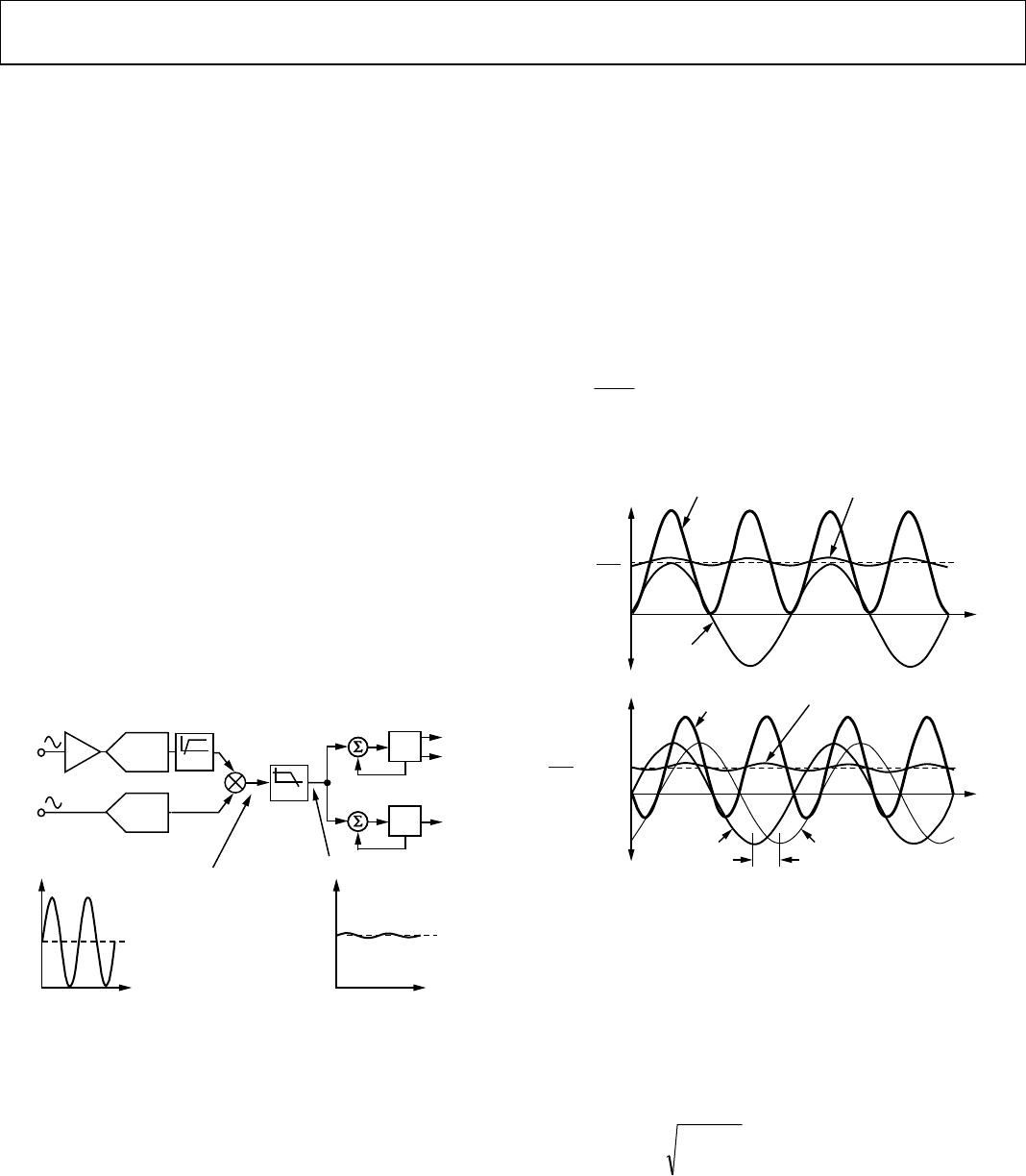
The real power calculation is derived from the instantaneous
power signal. The instantaneous power signal is generated by
a direct multiplication of the current and voltage signals. To
extract the real power component (the dc component), the
instantaneous power signal is low-pass filtered.
Figure 15
illustrates the instantaneous real power signal and shows how
the real power information can be extracted by low-pass
filtering the instantaneous power signal. This scheme correctly
calculates real power for sinusoidal current and voltage
waveforms at all power factors. All signal processing is carried
out in the digital domain for superior stability over temperature
and time.
TIME TIME
ADC
ADC
CH1
CH2
MULTIPLIER
F1
F2
DIGITAL-TO-
FREQUENCY
CF
DIGITAL-TO-
FREQUENCY
INSTANTANEOUS REAL
POWER SIGNAL
INSTANTANEOUS
POWER SIGNAL – p(t)
LPF
HPF
05332-005
Figure 15. Signal Processing Block Diagram
The low frequency outputs (F1 and F2) are generated by
accumulating this real power information. This low frequency
inherently means a long accumulation time between output
pulses. Consequently, the resulting output frequency is propor-
tional to the average real power. This average real power
information is then accumulated (by a counter) to generate real
energy information. Conversely, due to its high output frequen-
cy and shorter integration time, the CF output frequency is
proportional to the instantaneous real power. This is useful for
system calibration, which can be done faster under steady load
conditions.
Power Factor Considerations
The method used to extract the real power information from
the instantaneous power signal, that is, by low-pass filtering, is
still valid even when the voltage and current signals are not in
phase.
Figure 16 shows the unity power factor condition and a
displacement power factor (DPF) = 0.5, that is, current signal
lagging the voltage by 60°. Assuming that the voltage and
current waveforms are sinusoidal, the real power component of
the instantaneous power signal (that is, the dc term) is given by
(
°×
×
60cos
2
IV
)
(1)
This is the correct real power calculation.
V × I
2
0V
POWER
CURRENT
VOLTAGE
POWER
TIME
TIME
VOLTAGE CURRENT
V × I
2
COS (60°)
0V
INSTANTANEOUS
POWER SIGNAL
INSTANTANEOUS REAL
POWER SIGNAL
INSTANTANEOUS
POWER SIGNAL
INSTANTANEOUS REAL
POWER SIGNAL
60°
05332-006
Figure 16. DC Component of Instantaneous Power Signal Conveys
Real Power Information, PF < 1
Nonsinusoidal Voltage and Current
The real power calculation method also holds true for
nonsinusoidal current and voltage waveforms. All voltage
and current waveforms in practical applications have some
harmonic content. Using the Fourier transform, instantaneous
voltage and current waveforms can be expressed in terms of
their harmonic content.
(
h
0h
h
0
αtVVtv +××+=
sin2)(
)
(2)
where:
v(t) is the instantaneous voltage.
V
0
is the average value.
V
h
is the rms value of voltage harmonic h.
α
h
is the phase angle of the voltage harmonic.
ADE7769
Rev. A | Page 11 of 20
(
)
+××+=
oh
hh
O
βtIIti sin2)(
(3)
where:
i(t) is the instantaneous current.
I
0
is the dc component.
I
h
is the rms value of current harmonic h.
is the phase angle of the current harmonic.
h
β
Using Equations 2 and 3, the real power (P) can be expressed in
terms of its fundamental real power (P
1
) and harmonic real
power (P
H
) as P = P
1
+ P
H
where:
(4)
1111
IVP
φ
cos×=
111
βαφ
=
and
hh
1h
hH
IVP
φ
cos×=
(5)
hhh
βαφ
=
In Equation 5, a harmonic real power component is generated
for every harmonic, provided that harmonic is present in both
the voltage and current waveforms. The power factor calcu-
lation has previously been shown to be accurate in the case of a
pure sinusoid. Therefore, the harmonic real power must also
correctly account for the power factor because it is made up of
a series of pure sinusoids.
Note that the input bandwidth of the analog inputs is 7 kHz at
the nominal internal oscillator frequency of 450 kHz.
ANALOG INPUTS
Channel V1 (Current Channel)
The voltage output from the current sensor is connected to the
ADE7769 here. Channel V1 is a fully differential voltage input.
V1P is the positive input with respect to V1N.
The maximum peak differential signal on Channel V1 should
be less than ±30 mV (21 mV rms for a pure sinusoidal signal)
for specified operation.
+
30mV
30mV
V
CM
V1
DIFFERENTIAL INPUT
±30mV MAX PEAK
COMMON-MODE
±6.25mV MAX
V1P
V1N
V1
V
CM
AGND
05332-007
Figure 17. Maximum Signal Levels, Channel V1
Figure 17 shows the maximum signal levels on V1P and V1N.
The maximum differential voltage is ±30 mV. The differential
voltage signal on the inputs must be referenced to a common
mode, for example, AGND. The maximum common-mode
signal is ±6.25 mV, as shown in
Figure 17.
Channel V2 (Voltage Channel)
The output of the line voltage sensor is connected to the
ADE7769 at this analog input. Channel V2 is a fully differential
voltage input with a maximum peak differential signal of
±165 mV.
Figure 18 shows the maximum signal levels that can
be connected to the ADE7769 Channel V2.
+165mV
–165mV
V
CM
V2
DIFFERENTIAL INPUT
±165mV MAX PEAK
COMMON-MODE
±25mV MAX
V2P
V2N
V2
V
CM
AGND
05332-008
Figure 18. Maximum Signal Levels, Channel V2
Channel V2 is usually driven from a common-mode voltage,
that is, the differential voltage signal on the input is referenced
to a common mode (usually AGND). The analog inputs of the
ADE7769 can be driven with common-mode voltages of up to
25 mV with respect to AGND. However, best results are
achieved using a common mode equal to AGND.
Typical Connection Diagrams
Figure 19 shows a typical connection diagram for Channel V1.
A shunt is the current sensor selected for this example because
of its low cost compared to other current sensors, such as the
current transformer (CT). This IC is ideal for low current meters.
V1P
V1N
C
F
C
F
R
F
R
F
±30mV
SHUNT
AGND
PHASE NEUTRAL
05332-009
Figure 19. Typical Connection for Channel V1
Figure 20 shows a typical connection for Channel V2. Typically,
the ADE7769 is biased around the phase wire, and a resistor
divider is used to provide a voltage signal that is proportional to
the line voltage. Adjusting the ratio of R
A
, R
B
, and RB
F
is also a
convenient way of carrying out a gain calibration on a meter.

ADE7769ARZ-RL

Mfr. #:
Manufacturer:
Analog Devices Inc.
Description:
Data Acquisition ADCs/DACs - Specialized Energy Meter IC w/ Intg Oscillator
Lifecycle:
New from this manufacturer.
Delivery:
DHL FedEx Ups TNT EMS
Payment:
T/T Paypal Visa MoneyGram Western Union

Products related to this Datasheet