IDT1339
REAL-TIME CLOCK WITH SERIAL I
2
C INTERFACE RTC
IDT®
REAL-TIME CLOCK WITH SERIAL I
2
C INTERFACE 11
IDT1339 REV S 031014
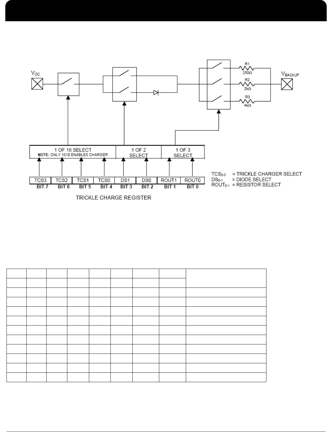
The user determines diode and resistor selection according to the maximum current desired for battery or super cap
charging. The maximum charging current can be calculated as illustrated in the following example. Assume that a 3.3 V
system power supply is applied to
V
CC
and a super cap is connected to V
BACKUP
. Also assume that the trickle charger has
been enabled with a diode and resistor R2 between
V
CC
and V
BACKUP
. The maximum current I
MAX
would therefore be
calculated as follows:
I
MAX
= (3.3 V - diode drop) / R2 (3.3 V - 0.7 V) / 2k 1.3 mA
As the super cap or battery charges, the voltage drop between
V
CC
and V
BACKUP
decreases and therefore the charge
current decreases.
I
2
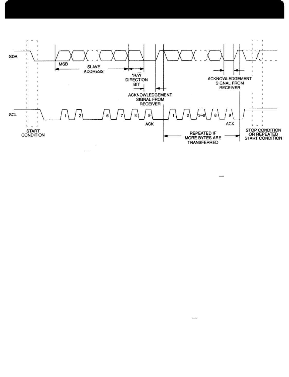
C Serial Data Bus
The IDT1339 supports the I
2
C bus protocol. A device that
sends data onto the bus is defined as a transmitter and a
device receiving data as a receiver. The device that controls
the message is called a master. The devices that are
controlled by the master are referred to as slaves. The bus
must be controlled by a master device that generates the
serial clock (SCL), controls the bus access, and generates
the START and STOP conditions. The IDT1339 operates as
a slave on the I
2
C bus. Within the bus specifications, a
standard mode (100 kHz cycle rate) and a fast mode (400
kHz cycle rate) are defined. The IDT1339 works in both
modes. Connections to the bus are made via the open-drain
I/O lines SDA and SCL.
The following bus protocol has been defined (see the “Data
Transfer on I
2
C Serial Bus” figure):
• Data transfer may be initiated only when the bus is not
busy.
• During data transfer, the data line must remain stable
whenever the clock line is HIGH. Changes in the data line
while the clock line is HIGH are interpreted as control
signals.
Accordingly, the following bus conditions have been defined:
Bus not busy: Both data and clock lines remain HIGH.
Start data transfer: A change in the state of the data line,
from HIGH to LOW, while the clock is HIGH, defines a
START condition.
Stop data transfer: A change in the state of the data line,
from LOW to HIGH, while the clock line is HIGH, defines the
STOP condition.
Data valid: The state of the data line represents valid data
when, after a START condition, the data line is stable for the
duration of the HIGH period of the clock signal. The data on
the line must be changed during the LOW period of the clock
signal. There is one clock pulse per bit of data.
Each data transfer is initiated with a START condition and
terminated with a STOP condition. The number of data
bytes transferred between START and STOP conditions is
not limited, and is determined by the master device. The
information is transferred byte-wise and each receiver
acknowledges with a ninth bit.
Acknowledge: Each receiving device, when addressed, is
obliged to generate an acknowledge after the reception of
each byte. The master device must generate an extra clock
pulse that is associated with this acknowledge bit.
A device that acknowledges must pull down the SDA line
during the acknowledge clock pulse in such a way that the
SDA line is stable LOW during the HIGH period of the
acknowledge related clock pulse. Of course, setup and hold
times must be taken into account. A master must signal an
end of data to the slave by not generating an acknowledge
bit on the last byte that has been clocked out of the slave. In
this case, the slave must leave the data line HIGH to enable
the master to generate the STOP condition.
Timeout: Timeout is where a slave device resets its
interface whenever Clock goes low for longer than the
timeout, which is typically 35mSec. This added logic deals
with slave errors and recovering from those errors. When
timeout occurs, the slave interface should re-initialize itself
and be ready to receive a communication from the master,
but it will expect a Start prior to any new communication.