IDT1339
REAL-TIME CLOCK WITH SERIAL I
2
C INTERFACE RTC
IDT®
REAL-TIME CLOCK WITH SERIAL I
2
C INTERFACE 4
IDT1339 REV S 031014
ESR (Effective Series Resistance)
Choose the crystal with lower ESR. A low ESR helps the
crystal to start up and stabilize to the correct output
frequency faster compared to high ESR crystals.
Frequency Tolerance
The frequency tolerance for 32kHz crystals should be
specified at nominal temperature (+25°C) on the crystal
manufacturer datasheet. The crystals used with IDT1339
typically have a frequency tolerance of ±20ppm at +25°C.
Specifications for a typical 32 kHz crystal used with our
device are shown in the table below.
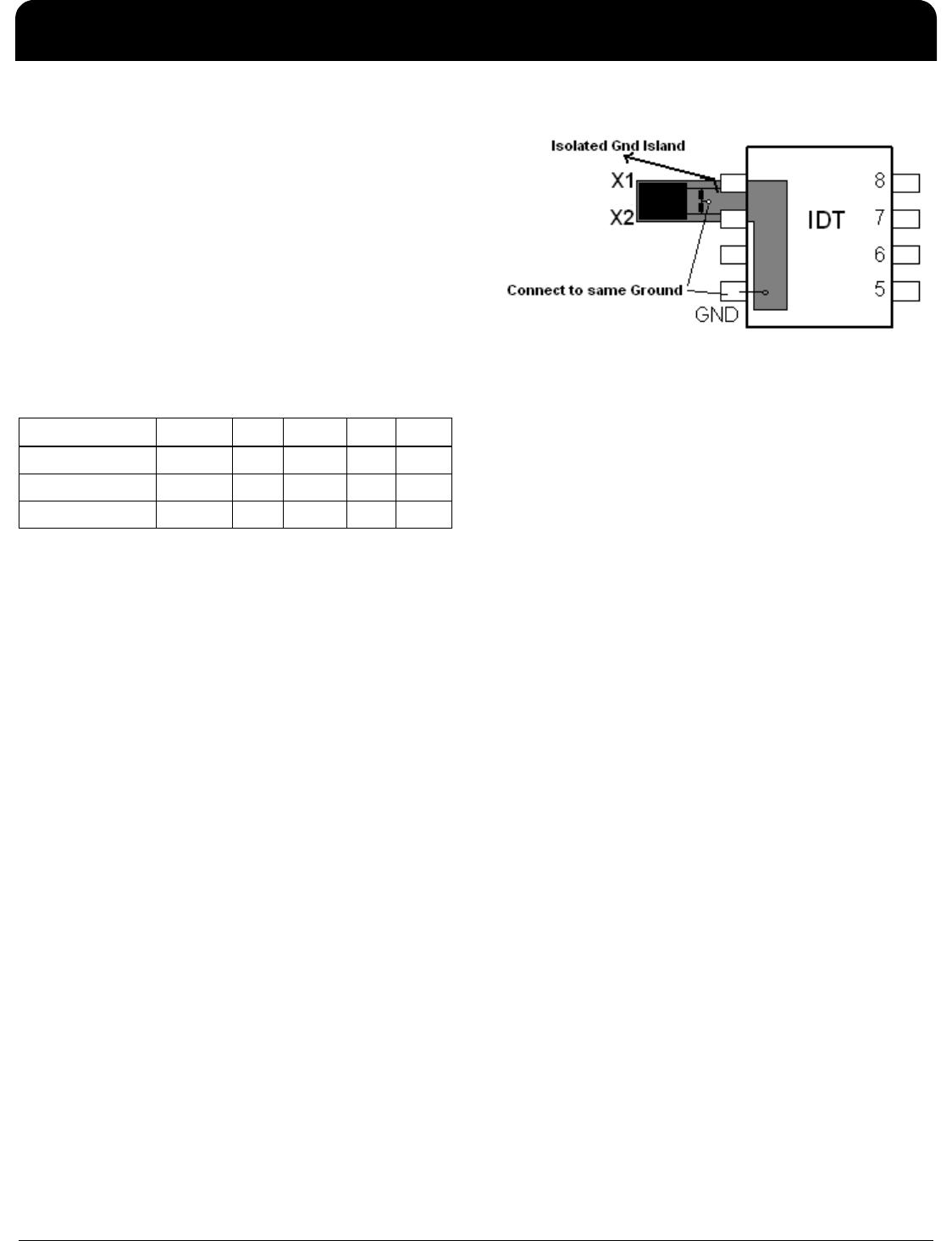
PCB Design Consideration
• Signal traces between IDT device pins and the crystal
must be kept as short as possible. This minimizes
parasitic capacitance and sensitivity to crosstalk and
EMI. Note that the trace capacitances play a role in the
effective crystal load capacitance calculation.
• Data lines and frequently switching signal lines should be
routed as far away from the crystal connections as
possible. Crosstalk from these signals may disturb the
oscillator signal.
• Reduce the parasitic capacitance between X1 and X2
signals by routing them as far apart as possible.
• The oscillation loop current flows between the crystal and
the load capacitors. This signal path (crystal to CL1 to
CL2 to crystal) should be kept as short as possible and
ideally be symmetric. The ground connections for both
capacitors should be as close together as possible.
Never route the ground connection between the
capacitors all around the crystal, because this long
ground trace is sensitive to crosstalk and EMI.
• To reduce the radiation / coupling from oscillator circuit,
an isolated ground island on the GND layer could be
made. This ground island can be connected at one point
to the GND layer. This helps to keep noise generated by
the oscillator circuit locally on this separated island. The
ground connections for the load capacitors and the
oscillator should be connected to this island.
PCB Layout
PCB Assembly, Soldering and Cleaning
Board-assembly production process and assembly quality
can affect the performance of the 32 kHz oscillator.
Depending on the flux material used, the soldering process
can leave critical residues on the PCB surface. High
humidity and fast temperature cycles that cause humidity
condensation on the printed circuit board can create
process residuals. These process residuals cause the
insulation of the sensitive oscillator signal lines towards
each other and neighboring signals on the PCB to decrease.
High humidity can lead to moisture condensation on the
surface of the PCB and, together with process residuals,
reduce the surface resistivity of the board. Flux residuals on
the board can cause leakage current paths, especially in
humid environments. Thorough PCB cleaning is therefore
highly recommended in order to achieve maximum
performance by removing flux residuals from the board after
assembly. In general, reduction of losses in the oscillator
circuit leads to better safety margin and reliability.
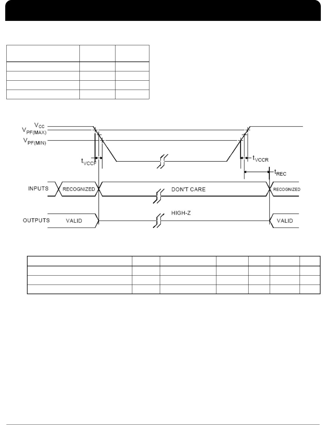
Power Control
The power-control function is provided by a precise,
temperature-compensated voltage reference and a
comparator circuit that monitors the
V
CC
level. The device is
fully accessible and data can be written and read when
V
CC
is greater than V
PF
. However, when V
CC
falls below V
PF
, the
internal clock registers are blocked from any access. If V
PF
is less than V
BACKUP
, the device power is switched from V
CC
to V
BACKUP
when V
CC
drops below V
PF
. If V
PF
is greater than
V
BACKUP
, the device power is switched from V
CC
to V
BACKUP
when
V
CC
drops below V
BACKUP
. The registers are
maintained from the V
BACKUP
source until V
CC
is returned to
nominal levels (Table 1). After
V
CC
returns above V
PF
, read
and write access is allowed after t
REC
(see the
“Power-Up/Down Timing” diagram).
Parameter Symbol Min Typ Max Units
Nominal Freq. f
O
32.768 kHz
Series Resistance ESR 50 k
Load Capacitance C
L
7pF