IDT1339
REAL-TIME CLOCK WITH SERIAL I
2
C INTERFACE RTC
IDT®
REAL-TIME CLOCK WITH SERIAL I
2
C INTERFACE 16
IDT1339 REV S 031014
AC Electrical Characteristics
Unless stated otherwise, V
CC
= MIN to MAX, Ambient Temperature -40 to +85C, Note 13
WARNING: Under no circumstances are negative undershoots, of any amplitude, allowed when device is in
battery-backup mode.
Note 1: Limits at -40°C are guaranteed by design and are not production tested.
Note 2: SCL only.
Note 3: SDA and SQW/INT
.
Note 4: I
CCA
—SCL at f
SC
max, VIL = 0.0V, VIH = V
CC
, trickle charger disabled.
Note 5: Specified with the I
2
C bus inactive, VIL = 0.0V, VIH = V
CC
, trickle charger disabled.
Note 6:
V
CC
must be less than 3.63 V if the 250 resistor is selected.
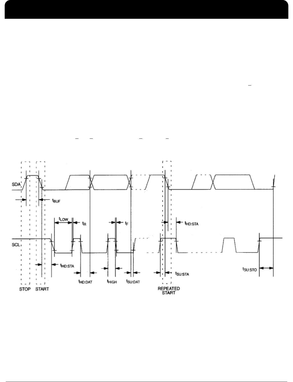
Parameter Symbol Conditions Min. Typ. Max. Units
SCL Clock Frequency f
SCL
Fast Mode 100 400 kHz
Standard Mode 100
Bus Free Time Between a STOP and
START Condition
t
BUF
Fast Mode 1.3 µs
Standard Mode 4.7
Hold Time (Repeated) START
Condition, Note 8
t
HD:STA
Fast Mode 0.6 µs
Standard Mode 4.0
Low Period of SCL Clock t
LOW
Fast Mode 1.3 µs
Standard Mode 4.7
High Period of SCL Clock t
HIGH
Fast Mode 0.6 µs
Standard Mode 4.0
Setup Time for a Repeated START
Condition
t
SU:STA
Fast Mode 0.6 µs
Standard Mode 4.7
Data Hold Time, Notes 9, 10 t
HD:DAT
Fast Mode 0 0.9 µs
Standard Mode 0
Data Setup Time, Note 11 t
SU:DAT
Fast Mode 100 ns
Standard Mode 250
Rise Time of Both SDA and SCL
Signals, Note 12
t
R
Fast Mode 20 + 0.1C
B
300 ns
Standard Mode 20 + 0.1C
B
1000
Fall Time of Both SDA and SCL Signals,
Note 12
t
F
Fast Mode 20 + 0.1C
B
300 ns
Standard Mode 20 + 0.1C
B
300
Setup Time for STOP Condition t
SU:STO
Fast Mode 0.6 µs
Standard Mode 4.0
Capacitive Load for Each Bus Line,
Note 12
C
B
400 pF
I/O Capacitance (SDA, SCL) C
I/O
Note 13 10 pF
Oscillator Stop Flag (OSF) Delay t
OSF
Note 14 100 ms
IDT1339
REAL-TIME CLOCK WITH SERIAL I
2
C INTERFACE RTC
IDT®
REAL-TIME CLOCK WITH SERIAL I
2
C INTERFACE 17
IDT1339 REV S 031014
Note 7: Using recommended crystal on X1 and X2.
Note 8: After this period, the first clock pulse is generated.
Note 9: A device must internally provide a hold time of at least 300 ns for the SDA signal (referred to the V
IHMIN
of
the SCL signal) to bridge the undefined region of the falling edge of SCL.
Note 10: The maximum t
HD:DAT
need only be met if the device does not stretch the LOW period (t
LOW
) of the SCL
signal.
Note 11: A fast-mode device can be used in a standard-mode system, but the requirement t
SU:DAT
> to 250 ns must
then be met. This is automatically the case if the device does not stretch the LOW period of the SCL signal. If such
a device does stretch the LOW period of the SCL signal, it must output the next data bit to the SDA line t
R(MAX)
+
t
SU:DAT
= 1000 + 250 = 1250 ns before the SCL line is released.
Note 12: C
B
—total capacitance of one bus line in pF.
Note 13: Guaranteed by design. Not production tested.
Note 14: The parameter t
OSF
is the period of time the oscillator must be stopped for the OSF flag to be set over the
voltage range of 0.0V <
V
CC
< V
CC
MAX and 1.3 V < V
BACKUP
< 3.7 V.
Timing Diagram
IDT1339
REAL-TIME CLOCK WITH SERIAL I
2
C INTERFACE RTC
IDT®
REAL-TIME CLOCK WITH SERIAL I
2
C INTERFACE 18
IDT1339 REV S 031014
Typical Operating Characteristics (V
CC
=3.3V, T
A
=25C)
Icc vs Vcc
(IDT1339-31)
SDA=GND
0
4
8
12
16
20
2.7 3.2 3.7 4.2 4.7 5.2
Supply current (uA)
Vcc (V)
SCL=400kHz
SCL=0Hz
IBACKUP vs Temperature
(IDT1339-31)
RS1=RS0=00
300
340
380
420
460
500
-40-200 20406080
Temperature (C)
Supply Current (nA)
INTC=1
INTC=0
Oscillator Frequency vs Supply Voltage
(IDT1339-31)
32768
32768.05
32768.1
2.8 3.3 3.8 4.3 4.8 5.3
Frequency (Hz)
Oscillator Supply Voltage (V)
Freq
IBACKUP vs VBACKUP
(IDT1339-31)
RS1=RS0=00
380
385
390
395
400
405
410
415
420
425
1.3 1.8 2.3 2.8 3.3
VBACKUP (V)
Supply Current (nA)
INTC=1
INTC=0

1339-2DCGI8

Mfr. #:
Manufacturer:
IDT
Description:
Real Time Clock RTC BASE
Lifecycle:
New from this manufacturer.
Delivery:
DHL FedEx Ups TNT EMS
Payment:
T/T Paypal Visa MoneyGram Western Union