Figure 3. SPI - transfer timing diagram
Figure 4. SPI - input timing
12345670
01
12345670
12345670
01
01
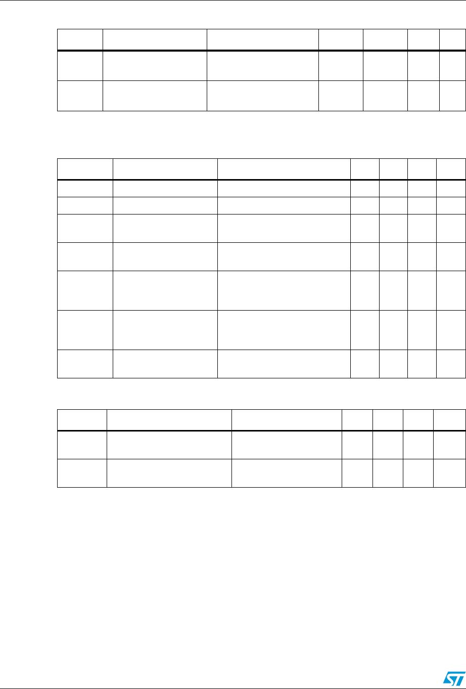
CSN
CLK
DI
DO
Input
Data
Register
CSN high to low: DO enabled
time
DI: data will be accepted on the rising edge of CLK signal
time
time
time
time
DO: data will change on the falling edge of CLK signal
fault bit
CSN low to high: actual data is
transfered to output power switches
old data new data
232221201918
232221201918
232221201918
X
X
XX
XX
12345670
01
12345670
12345670
01
12345670
12345670
01
01
CSN
CLK
DI
DO
Input
Data
Register
CSN high to low: DO enabled
time
DI: data will be accepted on the rising edge of CLK signal
time
time
time
time
DO: data will change on the falling edge of CLK signal
fault bit
CSN low to high: actual data is
transfered to output power switches
old data new data
232221201918
232221201918
232221201918
X
X
XX
XX