L9954LXP Block diagram and pin description
Doc ID 16186 Rev 3 7/35
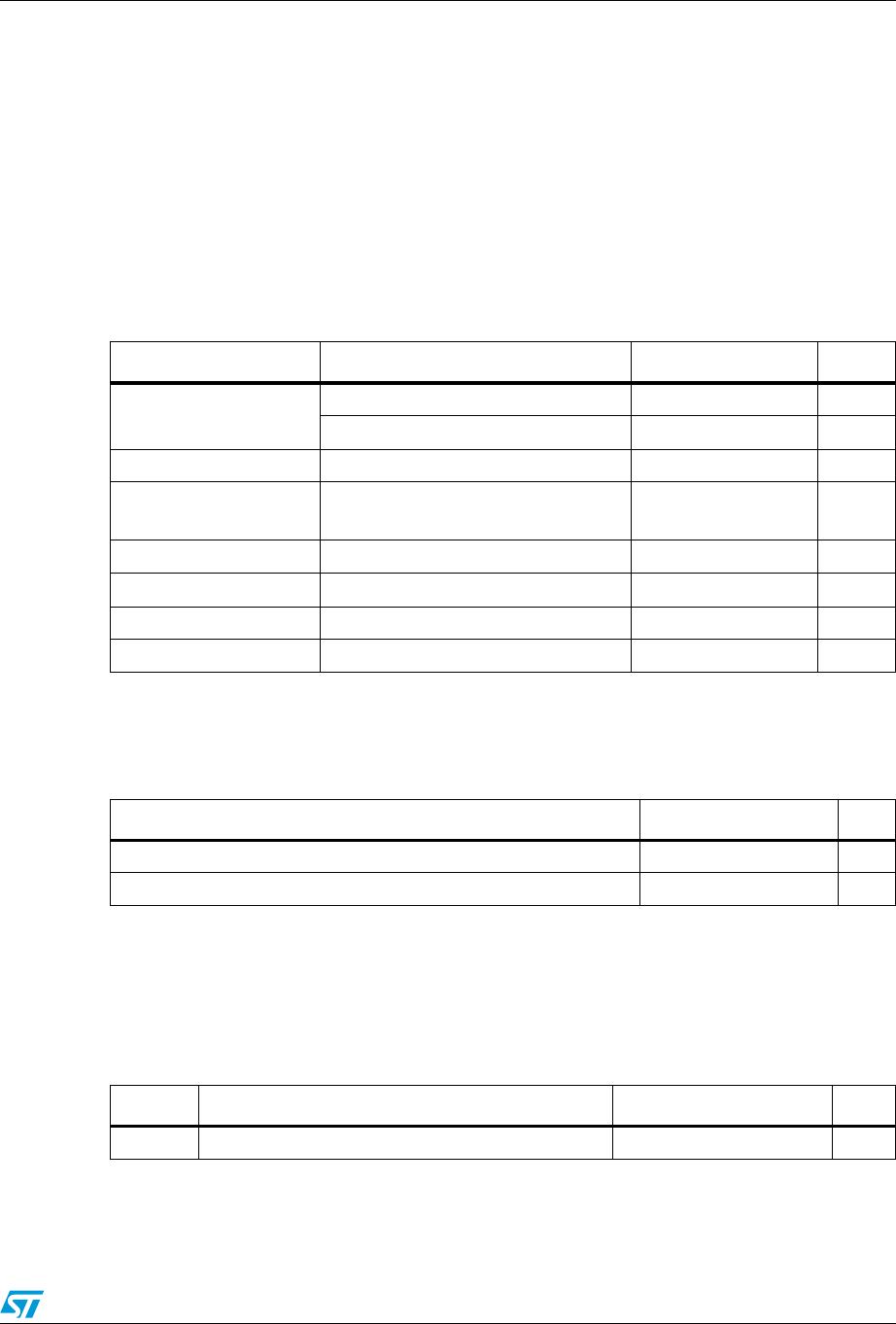
Table 2. Pin definitions and functions
Pin Symbol Function
1, 18, 19, 36 GND
Ground:
reference potential.
Important: for the capability of driving the full current at the outputs all
pins of GND must be externally connected.
2, 35 OUT6
High-side driver output 6
The output is built by a high-side switch and is intended for resistive
loads, hence the internal reverse diode from GND to the output is
missing. For ESD reason a diode to GND is present but the energy
which can be dissipated is limited. The high-side driver is a power
DMOS transistor with an internal parasitic reverse diode from the
output to V
S
(bulk-drain-diode). The output is over-current and open-
load protected.
Important: for the capability of driving the full current at the outputs both
pins of OUT6 must be externally connected.
3
4
5
OUT1
OUT2
OUT3
Half-bridge output 1,2,3
The output is built by a high-side and a low-side switch, which are
internally connected. The output stage of both switches is a power
DMOS transistor. Each driver has an internal parasitic reverse diode
(bulk-drain-diode: high-side driver from output to V
S
, switchs driver
from GND to output). This output is over-current and open-load
protected.
6, 7, 14, 25,
28, 32
V
S
Power supply voltage (external reverse protection required)
For this input a ceramic capacitor as close as possible to GND is
recommended.
Important: for the capability of driving the full current at the outputs all
pins of V
S
must be externally connected.
8DI
Serial data input
The input requires CMOS logic levels and receives serial data from the
microcontroller. The data is an 24bit control word and the least
significant bit (LSB, bit 0) is transferred first.
9 CM/PWM2
Current monitor output/PWM2 input
Depending on the selected multiplexer bits of input data register this
output sources an image of the instant current through the
corresponding high-side driver with a ratio of 1/10.000. This pin is
bidirectional. The microcontroller can overdrive the current monitor
signal to provide a second PWM input for the output OUT5.
10 CSN
Chip select not input
This input is low active and requires CMOS logic levels. The serial data
transfer between L9954LXP and micro controller is enabled by pulling
the input CSN to low-level.
11 DO
Serial data output
The diagnosis data is available via the SPI and this 3-state output. The
output remains in 3-state, if the chip is not selected by the input CSN
(CSN = high)