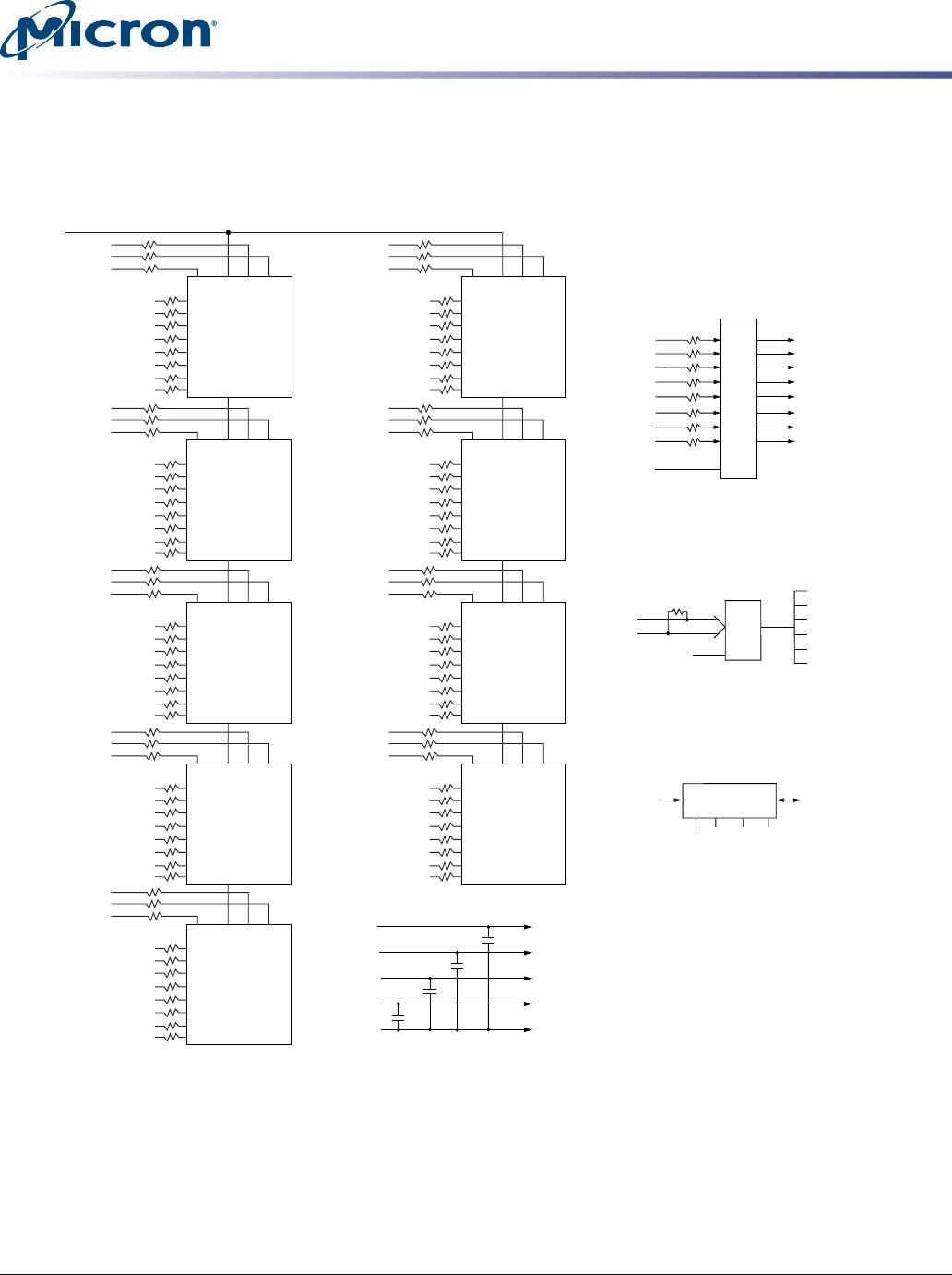
Pin Descriptions
The pin description table below is a comprehensive list of all possible pins for all DDR2
modules. All pins listed may not be supported on this module. See Pin Assignments for
information specific to this module.
Table 6: Pin Descriptions
Symbol Type Description
Ax Input Address inputs: Provide the row address for ACTIVE commands, and the column ad-
dress and auto precharge bit (A10) for READ/WRITE commands, to select one location
out of the memory array in the respective bank. A10 sampled during a PRECHARGE
command determines whether the PRECHARGE applies to one bank (A10 LOW, bank
selected by BAx) or all banks (A10 HIGH). The address inputs also provide the op-code
during a LOAD MODE command. See the Pin Assignments Table for density-specific
addressing information.
BAx Input Bank address inputs: Define the device bank to which an ACTIVE, READ, WRITE, or
PRECHARGE command is being applied. BA define which mode register (MR0, MR1,
MR2, and MR3) is loaded during the LOAD MODE command.
CKx,
CK#x
Input Clock: Differential clock inputs. All control, command, and address input signals are
sampled on the crossing of the positive edge of CK and the negative edge of CK#.
CKEx Input Clock enable: Enables (registered HIGH) and disables (registered LOW) internal circui-
try and clocks on the DDR2 SDRAM.
DMx Input Data mask (x8 devices only): DM is an input mask signal for write data. Input data
is masked when DM is sampled HIGH, along with that input data, during a write ac-
cess. Although DM pins are input-only, DM loading is designed to match that of the
DQ and DQS pins.
ODTx Input On-die termination: Enables (registered HIGH) and disables (registered LOW) termi-
nation resistance internal to the DDR2 SDRAM. When enabled in normal operation,
ODT is only applied to the following pins: DQ, DQS, DQS#, DM, and CB. The ODT input
will be ignored if disabled via the LOAD MODE command.
Par_In Input Parity input: Parity bit for Ax, RAS#, CAS#, and WE#.
RAS#, CAS#, WE# Input Command inputs: RAS#, CAS#, and WE# (along with S#) define the command being
entered.
RESET# Input Reset: Asynchronously forces all registered outputs LOW when RESET# is LOW. This
signal can be used during power-up to ensure that CKE is LOW and DQ are High-Z.
S#x Input Chip select: Enables (registered LOW) and disables (registered HIGH) the command
decoder.
SAx Input Serial address inputs: Used to configure the SPD EEPROM address range on the I
2
C
bus.
SCL Input Serial clock for SPD EEPROM: Used to synchronize communication to and from the
SPD EEPROM on the I
2
C bus.
CBx I/O Check bits. Used for system error detection and correction.
DQx I/O Data input/output: Bidirectional data bus.
DQSx,
DQS#x
I/O Data strobe: Travels with the DQ and is used to capture DQ at the DRAM or the con-
troller. Output with read data; input with write data for source synchronous opera-
tion. DQS# is only used when differential data strobe mode is enabled via the LOAD
MODE command.
512MB, 1GB (x72, ECC, SR) 244-Pin DDR2 SDRAM Mini-RDIMM
Pin Descriptions
PDF: 09005aef83f993e9
htf9c64_128x72pkz.pdf – Rev. C 4/14 EN
4
Micron Technology, Inc. reserves the right to change products or specifications without notice.
© 2010 Micron Technology, Inc. All rights reserved.
Table 6: Pin Descriptions (Continued)
Symbol Type Description
SDA I/O Serial data: Used to transfer addresses and data into and out of the SPD EEPROM on
the I
2
C bus.
RDQSx,
RDQS#x
Output Redundant data strobe (x8 devices only): RDQS is enabled/disabled via the LOAD
MODE command to the extended mode register (EMR). When RDQS is enabled, RDQS
is output with read data only and is ignored during write data. When RDQS is disa-
bled, RDQS becomes data mask (see DMx). RDQS# is only used when RDQS is enabled
and differential data strobe mode is enabled.
Err_Out# Output
(open drain)
Parity error output: Parity error found on the command and address bus.
V
DD
/V
DDQ
Supply Power supply: 1.8V ±0.1V. The component V
DD
and V
DDQ
are connected to the mod-
ule V
DD
.
V
DDSPD
Supply SPD EEPROM power supply: 1.7–3.6V.
V
REF
Supply Reference voltage: V
DD
/2.
V
SS
Supply Ground.
NC No connect: These pins are not connected on the module.
NF No function: These pins are connected within the module, but provide no functional-
ity.
NU Not used: These pins are not used in specific module configurations/operations.
RFU Reserved for future use.
512MB, 1GB (x72, ECC, SR) 244-Pin DDR2 SDRAM Mini-RDIMM
Pin Descriptions
PDF: 09005aef83f993e9
htf9c64_128x72pkz.pdf – Rev. C 4/14 EN
5
Micron Technology, Inc. reserves the right to change products or specifications without notice.
© 2010 Micron Technology, Inc. All rights reserved.
Functional Block Diagram
Figure 2: Functional Block Diagram
U1
A0
Serial PD
A1
A2
SA0
SA1
SA2
SDA
SCL
WP
DQ0
DQ1
DQ2
DQ3
DQ4
DQ5
DQ6
DQ7
DQ
DQ
DQ
DQ
DQ
DQ
DQ
DQ
DM/ CS# DQS DQS#
RDQS
DQ
DQ
DQ
DQ
DQ
DQ
DQ
DQ
DQ32
DQ33
DQ34
DQ35
DQ36
DQ37
DQ38
DQ39
RS0#
DQS0
DQS0#
DM0/DQS9
U6
DQS4
DQS4#
DM4/DQS13
DQS1
DQS1#
DM1/DQS10
DQS5
DQS5#
DM5/DQS14
DQS2
DQS2#
DM2/DQS11
DQS6
DQS6#
DM6/DQS15
DQS3
DQS3#
DM3/DQS12
DQS7
DQS7#
DM7/DQS16
DQS8
DQS8#
DM8/DQS17
DQ
DQ
DQ
DQ
DQ
DQ
DQ
DQ
DQ8
DQ9
DQ10
DQ11
DQ12
DQ13
DQ14
DQ15
DQ
DQ
DQ
DQ
DQ
DQ
DQ
DQ
DQ40
DQ41
DQ42
DQ43
DQ44
DQ45
DQ46
DQ47
U9
U12
DQ
DQ
DQ
DQ
DQ
DQ
DQ
DQ
DQ16
DQ17
DQ18
DQ19
DQ20
DQ21
DQ22
DQ23
DQ
DQ
DQ
DQ
DQ
DQ
DQ
DQ
DQ48
DQ49
DQ50
DQ51
DQ52
DQ53
DQ54
DQ55
DQ
DQ
DQ
DQ
DQ
DQ
DQ
DQ
DQ24
DQ25
DQ26
DQ27
DQ28
DQ29
DQ30
DQ31
DQ
DQ
DQ
DQ
DQ
DQ
DQ
DQ
DQ56
DQ57
DQ58
DQ59
DQ60
DQ61
DQ62
DQ63
DQ
DQ
DQ
DQ
DQ
DQ
DQ
DQ
CB0
CB1
CB2
CB3
CB4
CB5
CB6
CB7
U2
U3
U11
U8
U7
R
e
g
i
s
t
e
r
PLL
U10
S0#
BA[2/1:0]
A[13:0]
RAS#
CAS#
WE#
CKE0
ODT0
RESET#
RS0#: DDR2 SDRAM
RBA[2/1:0]: DDR2 SDRAM
RA[13:0]: DDR2 SDRAM
RRAS#: DDR2 SDRAM
RCAS#: DDR2 SDRAM
RWE#: DDR2 SDRAM
RCKE0: DDR2 SDRAM
RODT0: DDR2 SDRAM
CK0
CK0#
DDR2 SDRAM
DDR2 SDRAM
DDR2 SDRAM
DDR2 SDRAM
DDR2 SDRAM
Register
RESET#
U5
U4
V
REF
V
SS
DDR2 SDRAM
DDR2 SDRAM
V
DD
DDR2 SDRAM
V
DDSPD
Serial PD
V
DDQ
DDR2 SDRAM
DM/ CS# DQS DQS#
RDQS
DM/ CS# DQS DQS#
RDQS
DM/ CS# DQS DQS#
RDQS
DM/ CS# DQS DQS#
RDQS
DM/ CS# DQS DQS#
RDQS
DM/ CS# DQS DQS#
RDQS
DM/ CS# DQS DQS#
RDQS
DM/ CS# DQS DQS#
RDQS
V
SS
512MB, 1GB (x72, ECC, SR) 244-Pin DDR2 SDRAM Mini-RDIMM
Functional Block Diagram
PDF: 09005aef83f993e9
htf9c64_128x72pkz.pdf – Rev. C 4/14 EN
6
Micron Technology, Inc. reserves the right to change products or specifications without notice.
© 2010 Micron Technology, Inc. All rights reserved.

MT9HTF12872PKZ-80EH1

Mfr. #:
Manufacturer:
Micron
Description:
DRAM Module DDR2 SDRAM 1Gbyte 244MiniRDIMM
Lifecycle:
New from this manufacturer.
Delivery:
DHL FedEx Ups TNT EMS
Payment:
T/T Paypal Visa MoneyGram Western Union