12©2016 Integrated Device Technology, Inc. Revision D September 27, 2016
83905 Datasheet
Application Information
Crystal Input Interface
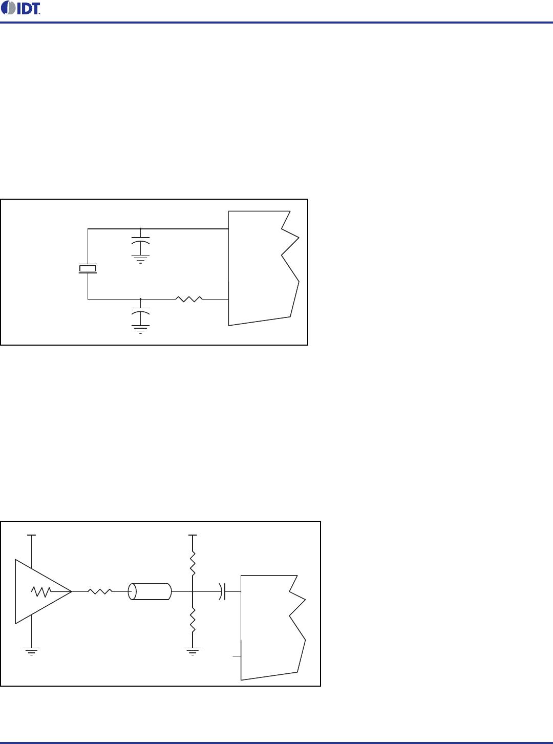
Figure 2 shows an example of 83905 crystal interface with a
parallel resonant crystal. The frequency accuracy can be fine
tuned by adjusting the C1 and C2 values. For a parallel crystal with
loading capacitance CL = 18pF, to start with, we suggest C1 =
15pF and C2 = 15pF. These values may be slightly fine tuned
further to optimize the frequency accuracy for different board
layouts. Slightly increasing the C1 and C2 values will slightly
reduce the frequency. Slightly decreasing the C1 and C2 values
will slightly increase the frequency. For the oscillator circuit below,
R1 can be used, but is not required. For new designs, it is
recommended that R1 not be used.
Figure 2. Crystal Input Interface
LVCMOS to XTAL Interface
The XTAL_IN input can accept a single-ended LVCMOS signal
through an AC coupling capacitor. A general interface diagram is
shown in Figure 3. The XTAL_OUT pin can be left floating. The
input edge rate can be as slow as 10ns. For LVCMOS inputs, it is
recommended that the amplitude be reduced from full swing to half
swing in order to prevent signal interference with the power rail and
to reduce noise. This configuration requires that the output
impedance of the driver (Ro) plus the series resistance (Rs) equals
the transmission line impedance. In addition, matched termination
at the crystal input will attenuate the signal in half. This can be
done in one of two ways. First, R1 and R2 in parallel should equal
the transmission line impedance. For most 50 applications, R1
and R2 can be 100. This can also be accomplished by removing
R1 and making R2 50. By overdriving the crystal oscillator, the
device will be functional, but note, the device performance is
guaranteed by using a quartz crystal.
Figure 3. General Diagram for LVCMOS Driver to XTAL Input Interface
XTAL_IN
XTAL_OUT
C1
15p
C2
15p
X1
18pF Parallel Crystal
R1 (optional)
0
XTAL_IN
XTAL_OUT
Ro Rs
Zo = Ro + Rs
50Ω
0.1µf
R1
R2
V
DD
V
DD